NROM flash memory devices on ultrathin silicon

a technology of ultrathin silicon and flash memory, applied in the field of memory devices, can solve the problems of increasing the speed of the transistor connection in relation to the speed of the transistor, and the soi technology imposes significant technical challenges, and it is difficult to make perfect crystalline silicon-on-oxide or silicon with other insulators

Active Publication Date: 2005-05-19
MICRON TECH INC
View PDF99 Cites 23 Cited by
  • Summary
  • Abstract
  • Description
  • Claims
  • Application Information

AI Technical Summary

Benefits of technology

[0008] The above-mentioned problems with eliminating floating body effects and other problems are addressed by the present invention and will be understood by reading and studying the following specification.

Problems solved by technology

However, as transistors are made smaller and faster, delays through the connections between the transistors becomes greater in relation to the speed of the transistor.
SOI technology, however, imposes significant technical challenges.
It is very difficult to make perfect crystalline silicon-on-oxide or silicon with other insulators since the insulator layer's crystalline properties are so different from the pure silicon.
If perfect crystalline silicon is not obtained, defects will find their way onto the SOI film.
This degrades the transistor performance.
Additionally, floating body effects in partially depleted CMOS devices using SOI technology are undesirable in many logic and memory applications.
In dynamic logic and DRAM memories, the floating bodies cause excess charge leakage and short retention times that can cause data loss.

Method used


Image

  • NROM flash memory devices on ultrathin silicon
  • NROM flash memory devices on ultrathin silicon
  • NROM flash memory devices on ultrathin silicon

Examples


Embodiment Construction

[0023] In the following detailed description of the invention, reference is made to the accompanying drawings that form a part hereof and in which is shown, by way of illustration, specific embodiments in which the invention may be practiced. In the drawings, like numerals describe substantially similar components throughout the several views. These embodiments are described in sufficient detail to enable those skilled in the art to practice the invention. Other embodiments may be utilized and structural, logical, and electrical changes may be made without departing from the scope of the present invention. The following detailed description is, therefore, not to be taken in a limiting sense, and the scope of the present invention is defined only by the appended claims and equivalents thereof.

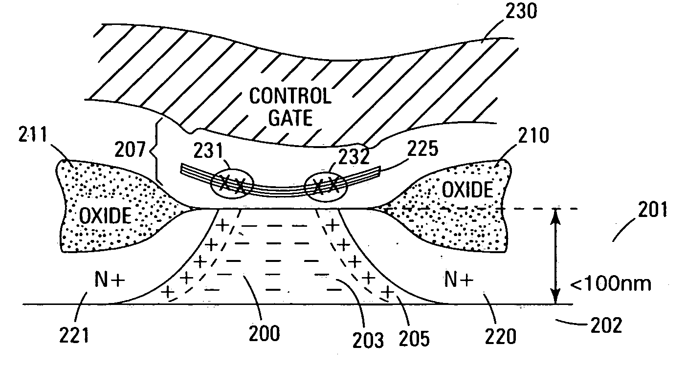
[0024]FIG. 2 illustrates a cross-sectional view of one embodiment of a planar NROM cell using ultra-thin silicon-on-insulator (SOD) technology. The NROM flash memory cell of FIG. 2 is a NOR arr...


PUM


Abstract

An NROM flash memory cell is implemented in an ultra-thin silicon-on-insulator structure. In a planar device, the channel between the source/drain areas is normally fully depleted. An oxide layer provides an insulation layer between the source/drain areas and the gate insulator layer on top. A control gate is formed on top of the gate insulator layer. In a vertical device, an oxide pillar extends from the substrate with a source/drain area on either side of the pillar side. Epitaxial regrowth is used to form ultra-thin silicon body regions along the sidewalls of the oxide pillar. Second source/drain areas are formed on top of this structure. The gate insulator and control gate are formed on top.

Description

TECHNICAL FIELD OF THE INVENTION [0001] The present invention relates generally to memory devices and in particular the present invention relates to nitride read only memory flash memory devices. BACKGROUND OF THE INVENTION [0002] The increased speed and capability of computers and other electronic devices requires better performance from the integrated circuits that make up a device. One way to make the integrated circuits faster is to reduce the size of the transistors that make up the device. However, as transistors are made smaller and faster, delays through the connections between the transistors becomes greater in relation to the speed of the transistor. [0003] An alternative technique to speed up integrated circuits is to use alternative semiconductors. For example, silicon-on-insulator (SOI) technology provides a 25-35% performance increase over equivalent CMOS technologies. SOI refers to placing a thin layer of silicon on top of an insulator such as silicon oxide or glass. ...

Claims


Application Information

Patent Timeline
Patent Type & Authority Applications(United States)
IPC IPC(8): H01L21/28H01L29/51H01L29/792H01L29/92
CPCH01L21/28211H01L21/84H01L27/115H01L27/11568H01L28/40H01L29/4234H01L29/7926H01L29/517H01L29/518H01L29/66833H01L29/78642H01L29/792H01L29/7923H01L29/513H10B69/00H10B43/30H01L21/76838
Inventor FORBES, LEONARD
Owner MICRON TECH INC
Why Eureka
Try Eureka