Superconductor with optimized microstructure and method for making such a superconductor

a superconductor and microstructure technology, applied in the direction of conductors, conductive materials, electrical equipment, etc., can solve the problems of cumbersome and costly processes for the fabrication of such superconductors, and achieve the effects of reducing manufacturing costs, reducing manufacturing costs, and reducing manufacturing costs

Inactive Publication Date: 2005-05-19
MANNHART JOCHEN DIETER
View PDF9 Cites 0 Cited by
  • Summary
  • Abstract
  • Description
  • Claims
  • Application Information

AI Technical Summary

Benefits of technology

[0024] Another advantage of the invention is that it simplifies the manufacturing process of superconductors for technical applications by allowing cheaper mass production of polycrystalline high-Tc and other superconductors with large critical current densities.
[0025] In the following, implementations of the invention shall be described, illustrated by the appended drawings.

Problems solved by technology

At present, the fabrication of such superconductors requires cumbersome and costly processes to optimize the grain boundary alignment.

Method used


Image

  • Superconductor with optimized microstructure and method for making such a superconductor
  • Superconductor with optimized microstructure and method for making such a superconductor
  • Superconductor with optimized microstructure and method for making such a superconductor

Examples


Embodiment Construction

AND EMBODIMENTS

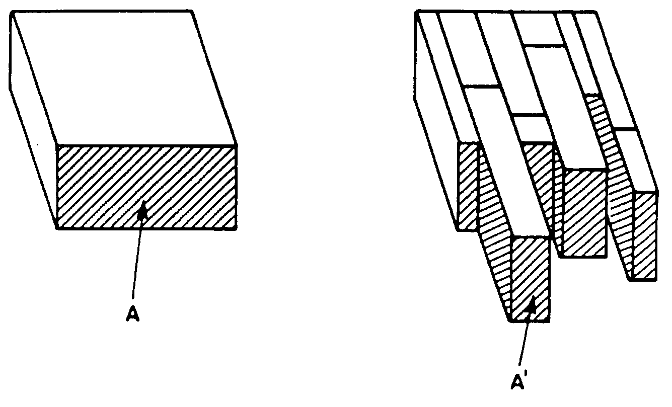
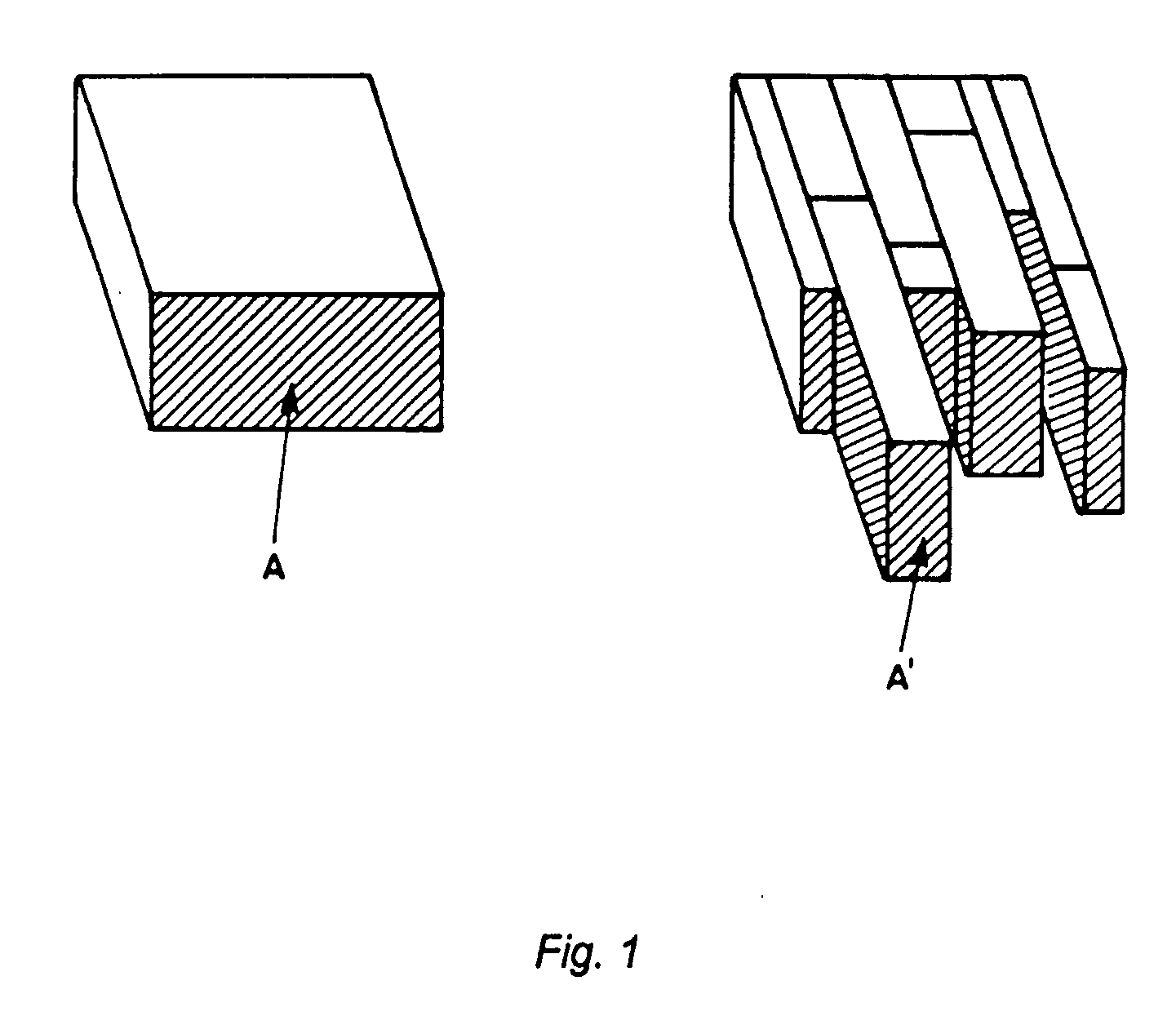
[0031] Because in the literature the term “grain” is used in a slightly confusing manner of coated conductors, we will clarify in the following the general usage to which we comply:

[0032] Standard RABiTS-tapes are described in the literature to consist of grains with a typical size of tens of micrometers. The growth structures out of which these grains consist are usually named “growth islands”.

[0033] In IBAD- and ISD-type tapes such grains are generally lacking. Therefore in these superconductors the only grain-like structures are the growth islands which usually are referred to as grains. Their boundaries limit the critical currents in these superconductors.

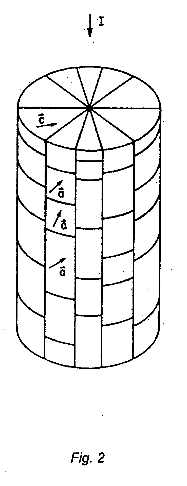
[0034] The enhancement of the critical current is also achieved in case the grains are tilted with respect to the substrate surface. For this case the length of the grain in the direction of the current flow and the width are defined according to FIG. 4.

[0035] We provide in the following examples for the fabr...


PUM

PropertyMeasurementUnit
misorientation angleaaaaaaaaaa
aspect ratioaaaaaaaaaa
Tc superconductorsaaaaaaaaaa

Abstract

The present invention concerns the improvement of the supercurrent carrying capabilities, i.e. the increase of critical current densities, of polycrystalline superconductor structures, especially of high-Tcsuperconductors. By modifying the microstructure of the substrate or by appropriately influencing the buffer layers in coated conductors to obtain grains with large aspect ratios which are predominantly oriented along the direction of the current flow, grain boundaries with large areas are obtained in the polycrystalline superconducting film that can support large critical currents along the superconductor. Thereby large critical currents are obtained in the superconductor for a given spread of misorientation angles of the grains.

Description

TECHNICAL FIELD [0001] The present invention relates to superconductors, particularly to the current carrying capabilities of superconductors. It is a proven fact that the critical currents of many superconductors, here polycrystalline superconductors, are limited by grain boundaries formed in them. The invention overcomes this limitation of present superconductors by using alterations for improving the current transport properties of the superconductors' grain boundaries. This is done in principle by optimizing the microstructure of the substrate or of a buffer layer system onto which the superconductor is deposited, such that the polycrystalline superconductor contains large grain boundary areas. BACKGROUND OF THE INVENTION [0002] Based on the new class of superconductors, henceforth referred to as high-Tc superconductors, which were discovered by Bednorz and Müller and disclosed in their article “Possible High-Tc Superconductivity in the Ba—La—Cu—O System”, Zeitschrift für Physik...

Claims


Application Information

Patent Timeline
Patent Type & Authority Applications(United States)
IPC IPC(8): H01L39/14H01L39/24
CPCH01L39/143Y10T29/49014H01L39/2454H10N60/203H10N60/0576
Inventor MANNHART, JOCHEN DIETER
Owner MANNHART JOCHEN DIETER
Why Eureka
Try Eureka