Method for manufacturing a semiconductor device

a manufacturing method and semiconductor technology, applied in the direction of transistors, electric devices, basic electric elements, etc., can solve the problem of difficult to form an even thickness gate insulating layer

Inactive Publication Date: 2005-05-26
SEIKO EPSON CORP
View PDF1 Cites 7 Cited by
  • Summary
  • Abstract
  • Description
  • Claims
  • Application Information

AI Technical Summary

Benefits of technology

[0016] In one aspect of the present invention, the method for manufacturing a semiconductor device may further include the following step before the step (b-4): forming a protective film so as to cover at least the insulating layer placed above a region in which the offset insulating layer is f...

Problems solved by technology

However, if a thick gate insulating layer for a high-voltage-proof transistor is formed on an offset insulating layer formed by STI, the gate insulating ...

Method used


Image

  • Method for manufacturing a semiconductor device
  • Method for manufacturing a semiconductor device
  • Method for manufacturing a semiconductor device

Examples


Embodiment Construction

[0044] One embodiment of the present invention will now be described.

[0045] First, the structure of a semiconductor device manufactured by a method for manufacturing a semiconductor device according to the present embodiment will be described.

[0046] Semiconductor device

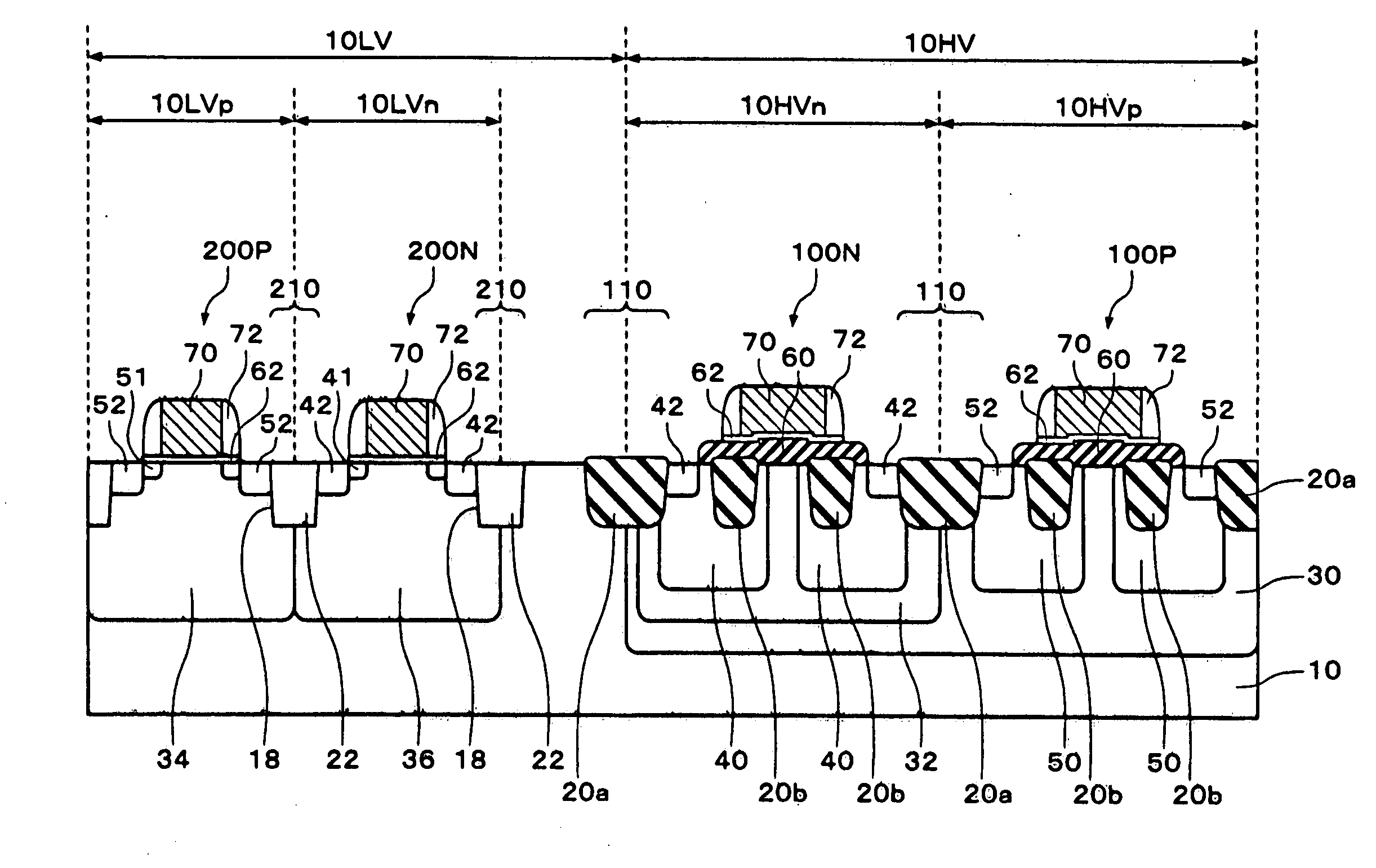
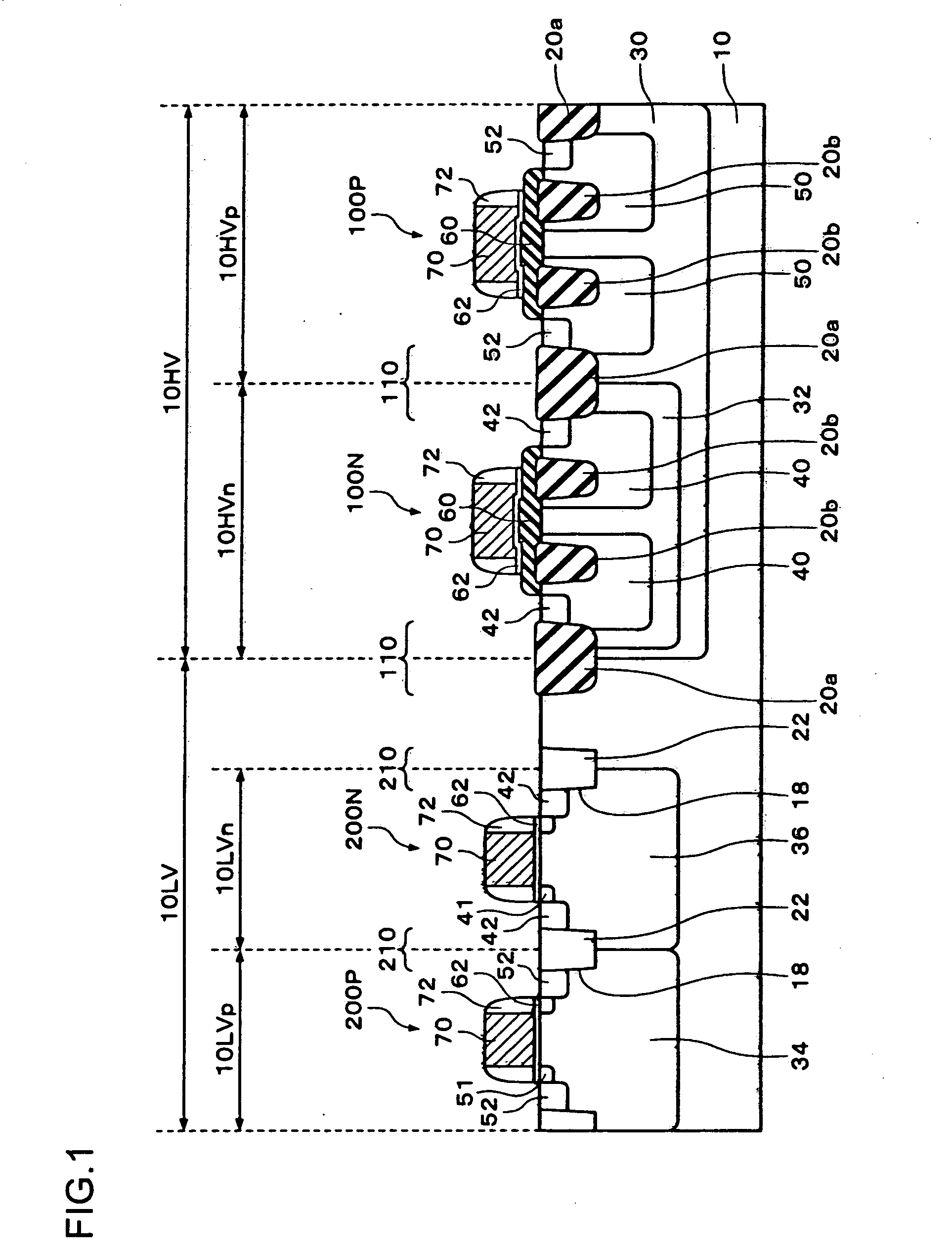
[0047]FIG. 1 is a sectional view schematically showing a semiconductor device manufactured by a method for manufacturing a semiconductor device according to the present embodiment. The semiconductor device manufactured by the method of the present embodiment includes high-voltage-proof transistors 100P and 100N (100P, N) and low-voltage-driven transistors 200P and 200N (200P, N) all of which are provided on a semiconductor substrate 10, which is a semiconductor layer. Provided in the semiconductor substrate 10 are a high-voltage-proof transistor region 10HV and a low-voltage-driven transistor region 10LV. The high-voltage-proof transistor region 10HV includes a P-channel high-voltage-proof transistor region 10HVp a...


PUM


Abstract

A semiconductor device manufacturing method includes: forming a first isolation region for setting a high-voltage-proof transistor forming region in a semiconductor layer; forming a second isolation region for setting a low-voltage-driven transistor forming region in the semiconductor layer by shallow-trench-isolation processing; and forming an offset insulating layer for electric field relaxation of high-voltage-proof transistors in the semiconductor layer by local-oxidation-of-silicon processing. The second step including: forming a trench in the semiconductor layer; forming an insulating layer filling up the trench and covering the entire upper surface of the semiconductor layer; removing part of the exposed insulating layer with a mask covering the insulating layer above a the offset insulating layer forming region and the trench forming region; removing at least the insulating layer in the high-voltage-proof transistor forming region by chemical-mechanical-polishing; and removing the insulating layer in the offset insulating layer forming region.

Description

RELATED APPLICATIONS [0001] This application claims priority to Japanese Patent Application No. 2003-370441 filed Oct. 30, 2003 which is hereby expressly incorporated by reference herein in its entirety. BACKGROUND [0002] 1. Technical Field [0003] The present invention relates to a method for manufacturing a semiconductor device having a high-voltage-proof transistor and a low-voltage-driven transistor that are provided on the same semiconductor layer, and more particularly to a method for manufacturing a semiconductor device employing both local oxidation of silicon (LOCOS) and shallow trench isolation (STI) processes. [0004] 2. Related Art [0005] A field-effect transistor having a LOCOS offset-structure has been proposed to withstand high voltages. The field-effect transistor having a LOCOS offset structure is a transistor having a LOCOS layer provided between a gate insulating layer and a drain region, and also having an offset impurity layer provided under the LOCOS layer. In ma...

Claims


Application Information

Patent Timeline
IPC IPC(8): H01L21/76H01L21/762H01L21/316H01L21/8234H01L21/8238H01L27/092
CPCH01L21/76202H01L21/76224H01L21/823481H01L21/823462H01L21/823418
Inventor KASUYA, YOSHIKAZU
Owner SEIKO EPSON CORP
Why Eureka
Try Eureka