Method and structure for controlled impedance wire bonds using co-dispensing of dielectric spacers

a dielectric spacer and controlled impedance technology, applied in the field of wire bonding, can solve the problems of inefficiency, inapplicability in all cases, and ineffective implementation of existing solutions, so as to reduce product costs, reduce cost, and increase data rate

Inactive Publication Date: 2005-06-02
GLOBALFOUNDRIES INC
View PDF13 Cites 32 Cited by
  • Summary
  • Abstract
  • Description
  • Claims
  • Application Information

AI Technical Summary

Benefits of technology

[0016] The present invention provides a technique in which product costs can be reduced without a sacrifice in electrical performance. Improved signal transmission at higher data rates permitted by this invention will allow lower cost bond wire tec...

Problems solved by technology

Although these solutions work, they are not applicable in all cases.
For example, these solutions are not efficient in the sense that the high frequency signals in the transition might involve only a few of the intercon...

Method used


Image

  • Method and structure for controlled impedance wire bonds using co-dispensing of dielectric spacers
  • Method and structure for controlled impedance wire bonds using co-dispensing of dielectric spacers
  • Method and structure for controlled impedance wire bonds using co-dispensing of dielectric spacers

Examples


Embodiment Construction

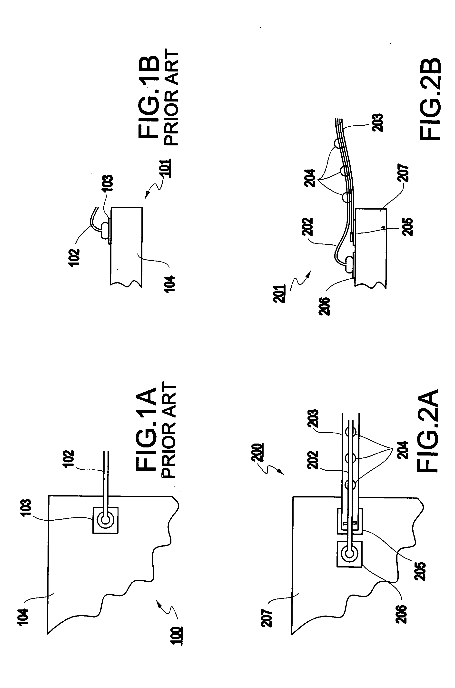
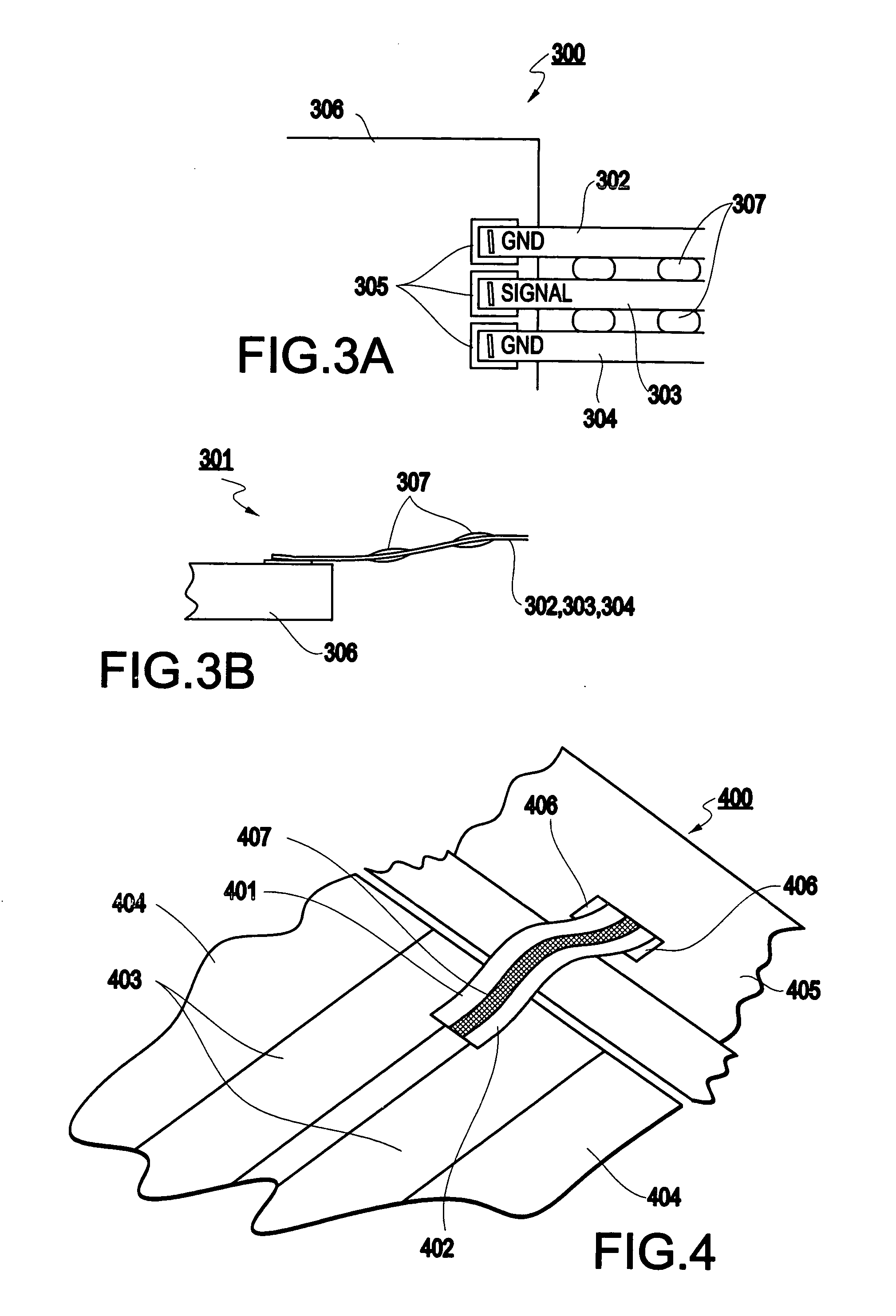
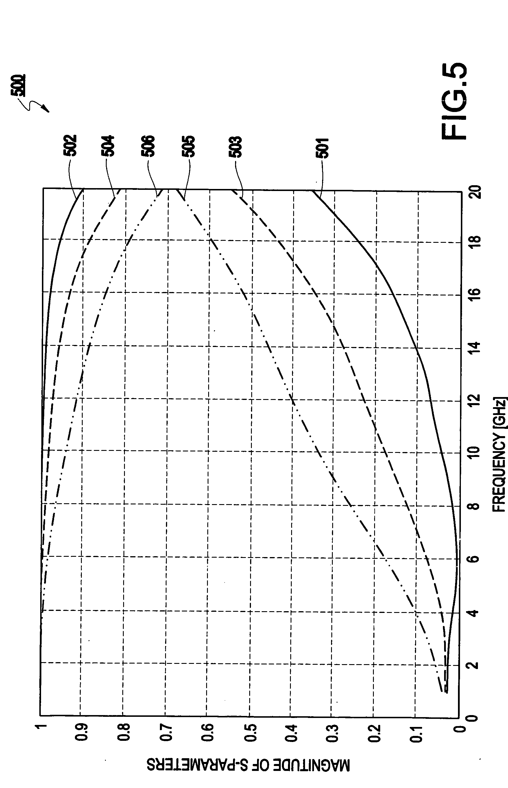
[0023] Referring now to the drawings, and more particularly to FIGS. 2A-5, exemplary embodiments of the present invention will now be described.

[0024] It is noted that one of ordinary skill in the art, after having read the details described herein, would readily be able to apply the present invention as a method of producing a transition for a chip to interconnect the chip to terminals of a package, interconnecting chips within a package, interconnecting a chip to a board, or otherwise interconnecting the chip.

[0025] However, although the present invention is discussed in the environment of a chip transition, there is no intent that it be thus limited, since one of ordinary skill in the art would readily recognized that the concept can be generalized as applying more generically (e.g., to electronic interconnections).

[0026] That is, the present invention can equally be applied to, for example, to integrated circuits, semiconductor devices, passive devices, filters, and so on.

[0...


PUM


Abstract

A method (and structure) of making an electronic interconnection, includes, for a signal line to be interconnected, using a plurality of bonding wires configured to provide a controlled impedance effect.

Description

BACKGROUND OF THE INVENTION [0001] 1. Field of the Invention [0002] The present invention generally relates to wire bonding of devices to the next level of packaging or between devices within a package. More specifically, to improve wide bandwidth signal transmission, the parasitic inductance can be lowered and compensated with distributed capacitance by tightly spacing a plurality of bond wires and / or bond ribbons so that the resulting impedance can be controlled for wide bandwidth signal transmission. [0003] 2. Description of the Related Art [0004] Transition of signals between a device and the next level of packaging (e.g., a semiconductor device and package), or between devices is often achieved by using bond wires (also referred to herein as bonding wires). FIG. 1A shows a top view 100 and FIG. 1B shows a side view 101 of a typical round wire bonding technique. In this example, round wire 102 is bonded to pad 103 mounted on chip 104. SUMMARY OF THE INVENTION [0005] Bond wires c...

Claims


Application Information

Patent Timeline
IPC IPC(8): H01L23/66H05K1/02
CPCH01L23/66H01L2224/49174H01L24/45H01L24/46H01L24/48H01L24/50H01L24/73H01L2223/6611H01L2223/6627H01L2224/43H01L2224/45014H01L2224/45124H01L2224/45144H01L2224/48465H01L2224/48599H01L2224/48699H01L2224/8502H01L2924/01005H01L2924/01006H01L2924/01013H01L2924/01027H01L2924/01079H01L2924/09701H01L2924/14H01L2924/1903H01L2924/30105H01L2924/30107H01L2924/3011H05K1/0219H05K1/0243H05K2201/0792H05K2201/09236H05K2201/1028H05K2203/049H01L24/43H01L2924/01033H01L2924/00014H01L2924/00H01L2924/15787H01L2924/30111H01L24/49H01L24/86H01L2224/45015H01L2224/49051H01L2224/85399H01L2224/05599H01L2924/206
Inventor KWARK, YOUNG HOONSCHUSTER, CHRISTIAN
Owner GLOBALFOUNDRIES INC
Why Eureka
Try Eureka