Module for contactless chip cards or identification systems

a technology of contactless chip cards and modules, applied in semiconductor devices, semiconductor/solid-state device details, instruments, etc., can solve the problem that the acrylate film required for fixing contributes directly to the total thickness of the module, and achieves the effect of sufficient robustness and stability

Active Publication Date: 2005-06-02
INFINEON TECH AG
View PDF5 Cites 0 Cited by
  • Summary
  • Abstract
  • Description
  • Claims
  • Application Information

AI Technical Summary

Benefits of technology

[0007] It is an object of the present invention to provide a module for contactless chip cards or identification systems which is thin...

Problems solved by technology

It has proven disadvantageous in a module produced by this process that the acrylate...

Method used


Image

  • Module for contactless chip cards or identification systems
  • Module for contactless chip cards or identification systems

Examples


Embodiment Construction

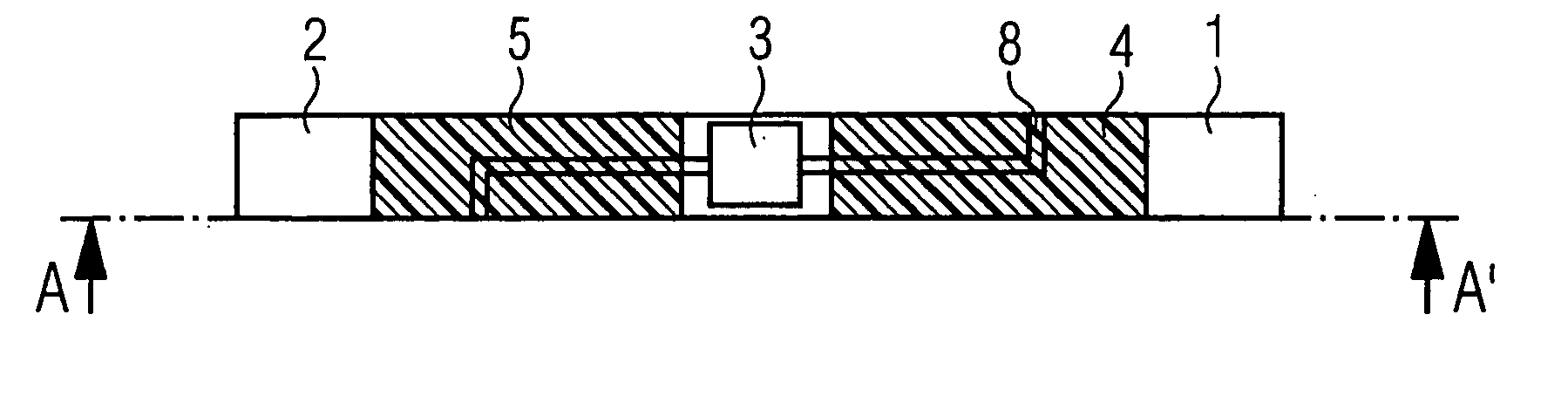
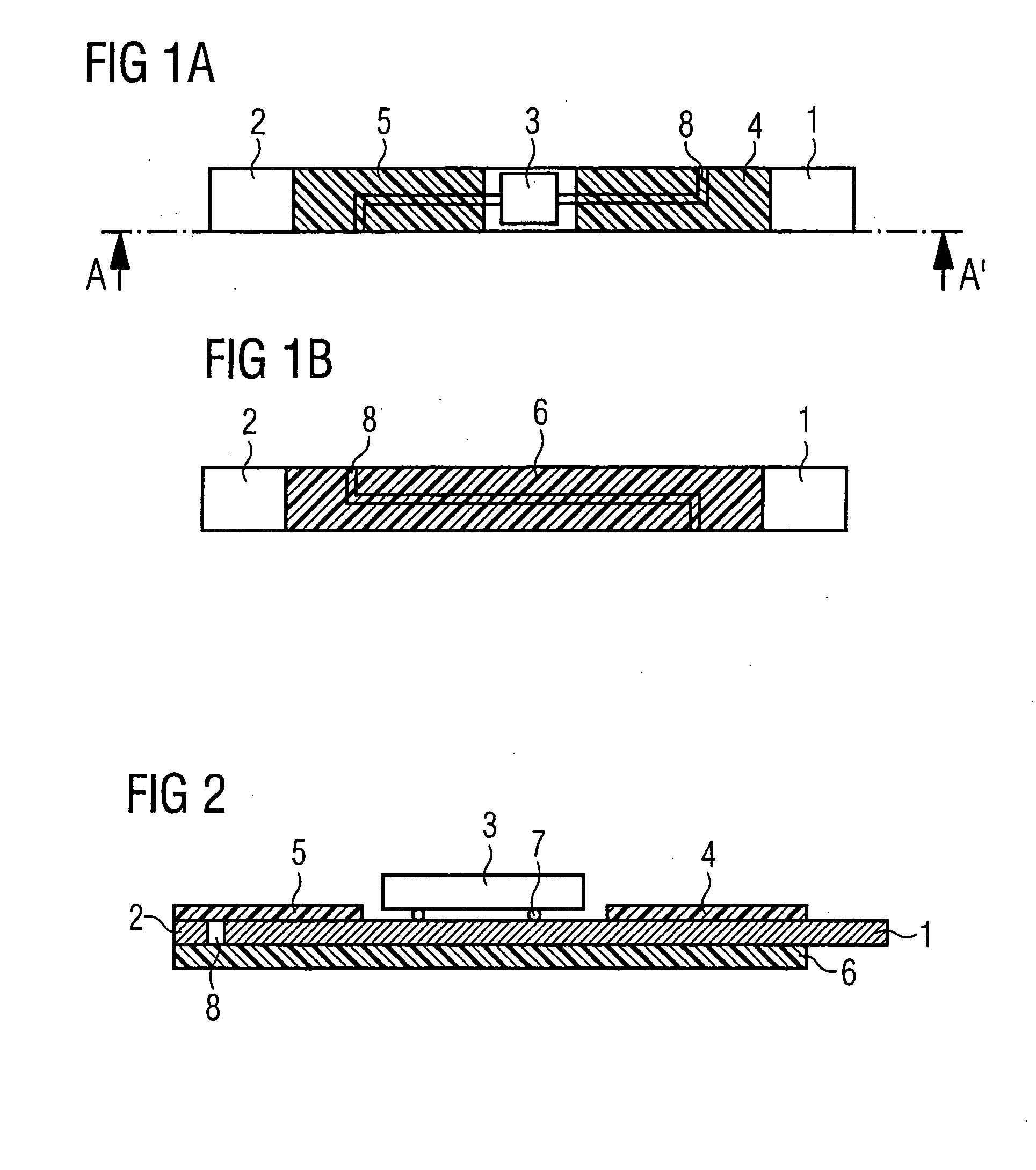
[0024]FIG. 1A illustrates a diagrammatic plan view of the front surface of a module configured in accordance with the invention, revealing a first antenna contact strip 1 and a—-second antenna contact strip 2. The first antenna contact strip 1 and the second antenna contact strip 2 are in each case composed of a wide antenna connection zone and a narrow, finger-shaped chip land zone, the chip land zone being longer than the antenna connection zone.

[0025] The first antenna contact strip 1 and the second antenna contact strip 2 are arranged in such a way that the chip land zone of the first antenna contact strip 1 and the chip land zone of the second antenna contact strip 2 are located next to one another and run parallel over their length. A spacing 8 is formed between the first antenna contact strip 1 and the second antenna contact strip 2.

[0026] A semiconductor chip 3, which extends from the chip land zone of the first antenna contact strip 1 to the chip land zone of the second a...


PUM


Abstract

Module for contactless chip cards or identification systems having a first antenna contact strip and a second antenna contact strip, which each have a first surface and a second surface facing away from the first surface, a semiconductor chip with at least two contacts, at least one contact contact-connecting the first surface of the first antenna contact strip and at least one further contact contact-connecting the first surface of the second antenna contact strip, and at least one adhesive film strip, which at least partially covers the first surface of both the first antenna contact strip and the second antenna contact strip, the at least one adhesive film strip being arranged outside a region of the first and second antenna contact strips that is covered by the semiconductor chip.

Description

CROSS-REFERENCE TO RELATED APPLICATION [0001] This application claims priority to German Patent Application Serial No. 10356153.6, filed Dec. 2, 2003, and which-is-incorporated herein by reference in its entirety. FIELD OF THE INVENTION [0002] The invention relates to a module for contactless chip cards or identification systems. BACKGROUND OF THE INVENTION [0003] Such modules for contactless chip cards or identification systems are known per se, for example under designation MCC2 from Infineon Technologies AG. One possible process for producing these modules is also known from patent application WO 96 / 05614. [0004] It is to be considered an important factor of this known production process that a chip with contact bumps is fixed by an acrylate film located on a leadframe. The contact bumps are pressed through the film and contact-connected to the leadframe by diffusion soldering. The acrylate film is located between the chip and the leadframe. [0005] It has proven disadvantageous i...

Claims


Application Information

Patent Timeline
IPC IPC(8): G06K19/06G06K19/077H01L21/56H01L23/485
CPCG06K19/07747H01L2924/0102H01L2224/16G06K19/07749
Inventor PUSCHNER, FRANKMULLER-HIPPER, ANDREASKARL, ANDREAS
Owner INFINEON TECH AG
Why Eureka
Try Eureka