Active matrix substrate, display apparatus, and method for producing the same

a technology of active matrix substrate and display apparatus, which is applied in the direction of identification means, instruments, optics, etc., can solve the problems of reducing the risk of defective display, serious production yield problems, and scattered pieces of conductive materials, so as to prevent prevent the effect of a conductive layer from bulging

Inactive Publication Date: 2005-06-02
SHARP KK
View PDF16 Cites 24 Cited by
  • Summary
  • Abstract
  • Description
  • Claims
  • Application Information

AI Technical Summary

Benefits of technology

[0025] According to one aspect of the invention, an active matrix substrate for allowing a point defeat of a defect pixel portion, among a plurality of pixel portions arranged two-dimensionally, to be repaired by radiation of energy is provided. The active matrix substrate includes one of a first protection member for absorbing excessive energy p

Problems solved by technology

The user recognizes this as a point-like pixel defect (hereinafter, referred to as the “point defect”) on the display screen such a point defect significantly spoils the display quality of the liquid crystal display apparatus, and is a serious problem in terms of production yield.
One type of defect is an ON defect.
This decreases the risk of a defective display due to the disturbance of the alignment layers an

Method used


Image

  • Active matrix substrate, display apparatus, and method for producing the same
  • Active matrix substrate, display apparatus, and method for producing the same
  • Active matrix substrate, display apparatus, and method for producing the same

Examples


example 1

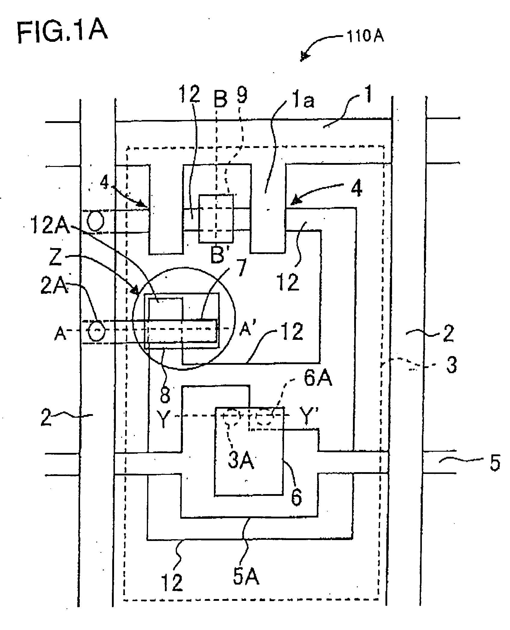
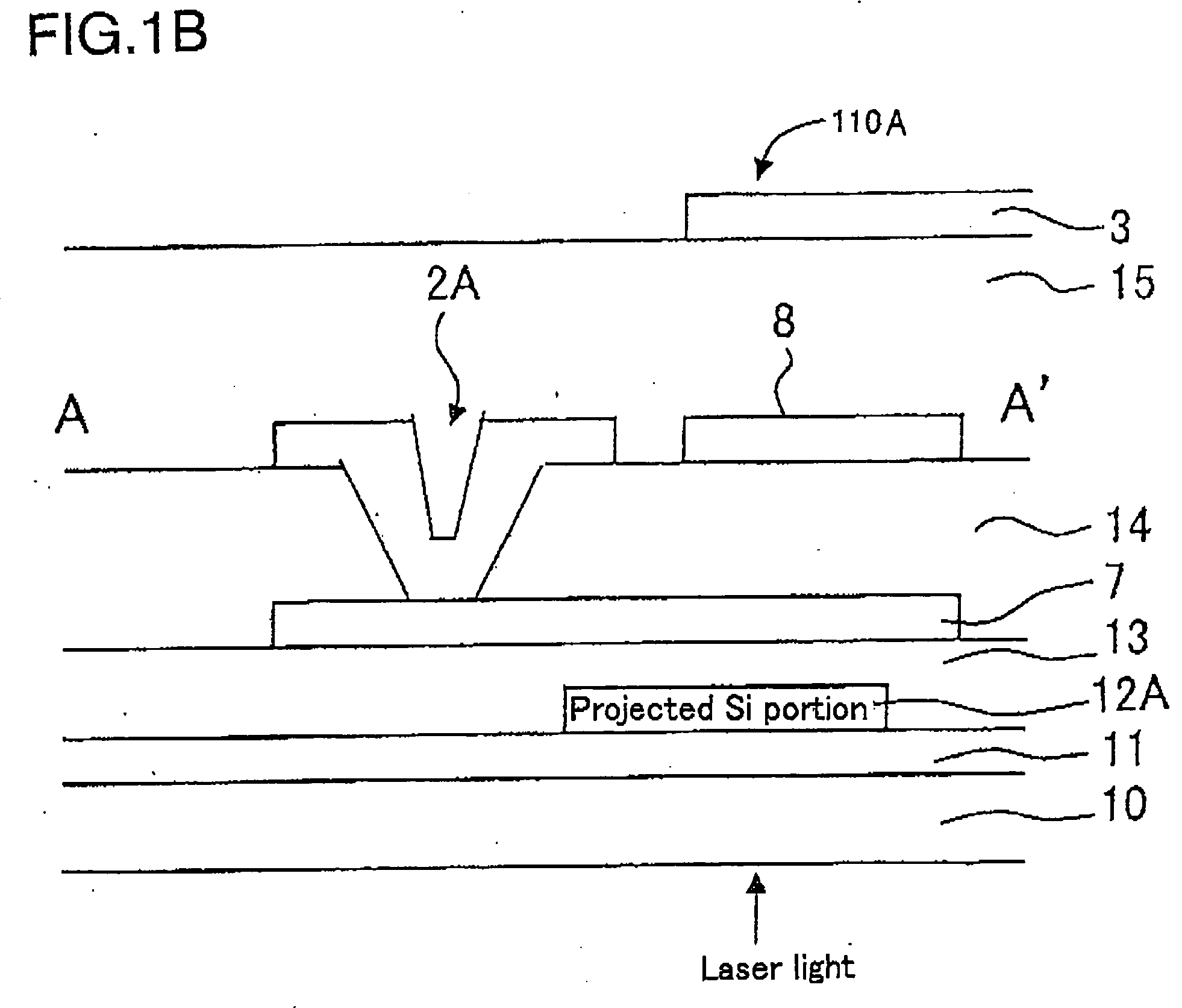
[0106] An active matrix liquid crystal display apparatus 110 (FIG. 3A) according to Example 1 of the present invention includes a pair of substrates facing each other with a liquid crystal layer interposed therebetween. FIG. 1A is a plan view of one of the substrates, i.e., an active matrix substrate 110A. More specifically, FIG. 1A shows a single display unit of the active matrix substrate 110A. FIG. 1B is a cross-sectional view of a part of FIG. 1A taken along line A-A′. Elements which are substantially the same as those in FIGS. 32A through 32C bear identical reference numerals therewith and will not be described in detail here. An overlapping portion of the gate region 1a and the semiconductor layer 12 acts as a control region.

[0107] The following description regarding the structure of an active matrix liquid crystal display apparatus according to the present invention will be concerned with a single display unit unless otherwise specified, throughout this specification.

[0108]...

example 2

[0180] In Example 2 according to the present invention, a spacer member (PS) for adjusting the distance between the active matrix substrate and the counter substrate of an active matrix liquid crystal display apparatus is provided above the laser radiation portion so as to be used also for repairing a point defect. The spacer member acts to prevent pieces of the conductive material from being scattered and to prevent the conductive layer from bulging.

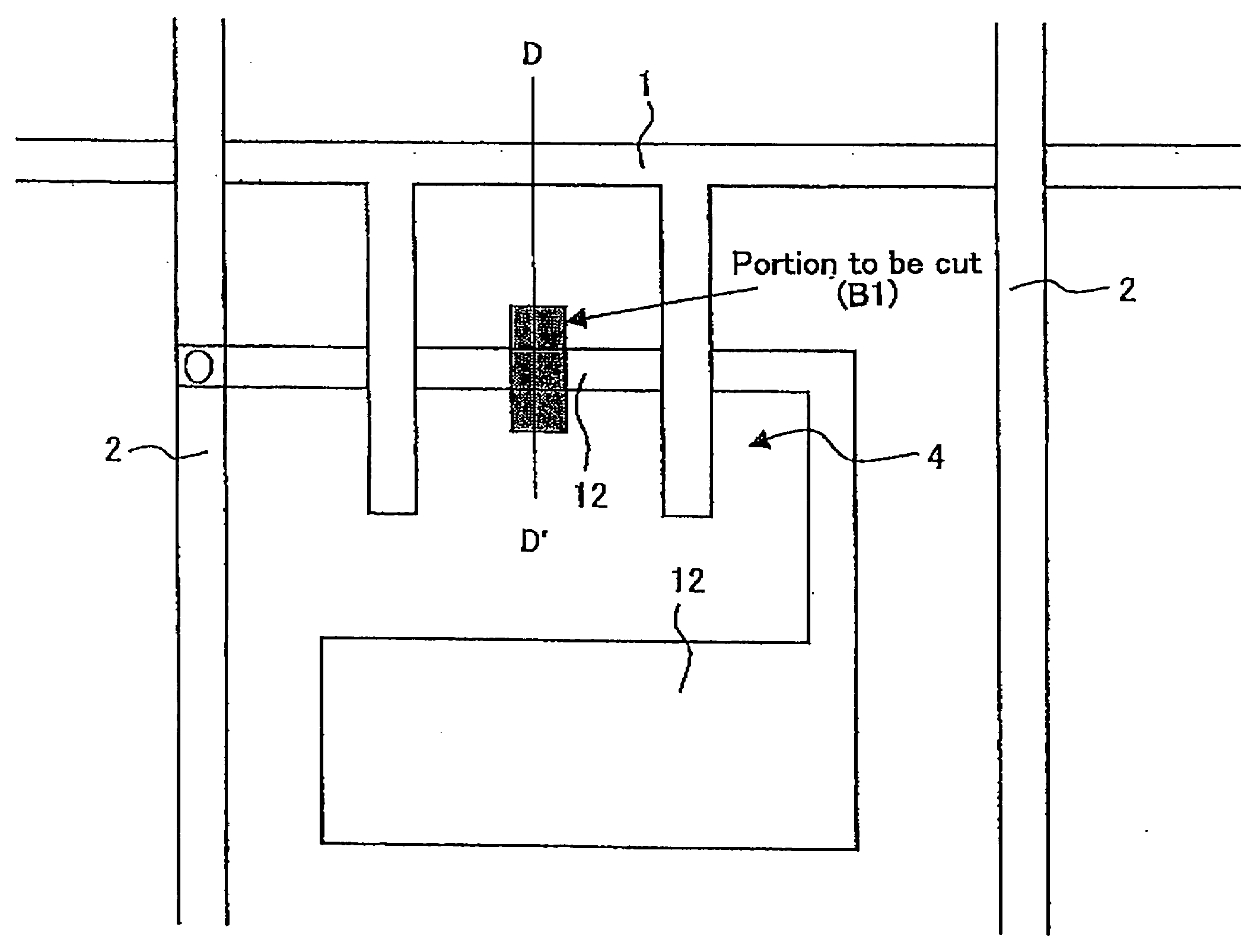
[0181]FIG. 16 shows a portion C1 to be cut in an active matrix liquid crystal display apparatus according to Example 2 of the present invention. The portion C1 is between the gates of the two TFTs 4 of an active matrix substrate of the active matrix liquid crystal display apparatus. FIG. 17A is a partial cross-sectional view of FIG. 16 taken along line C-C′. FIG. 18 shows a portion C1 to be cut in an active matrix liquid crystal display apparatus in a reference example. FIG. 19 is a partial cross-sectional view of FIG. 18 taken a long ...

example 3

[0204] In Example 3 according to the present invention, a spacer member (PS) 82 is provided on the counter substrate.

[0205]FIGS. 26 and 27 are each a cross-sectional views of an active matrix liquid crystal display apparatus according to Example 3 of the present invention. The cross-sectional views in FIGS. 26 and 27 correspond to the cross-sectional view taken along line C-C′ in FIG. 16.

[0206] In Example 3, as shown in FIGS. 26 and 27, the spacer member (PS) 82 is provided above the laser radiation portion for cutting (corresponding to the portion C1 in FIG. 16). The spacer member (PS) 82 is provided on the counter substrate (color filter substrate).

[0207] In the case where the spacer member (PS) 82 is formed of a resin, the spacer member (PS) 82 is provided by adding an additional step of forming a resin layer to the production method of the counter substrate. This step is added before the counter electrode 41 is formed (FIG. 26; the spacer member (PS) 82 is formed on the glass...


PUM


Abstract

In an active matrix substrate for allowing a point defect of a defect pixel portion, among a plurality of pixel portions arranged two-dimensionally, to be repaired by radiation of energy, the active matrix substrate includes one of a first protection member for absorbing excessive energy power and preventing pieces of a conductive material from being scattered; and a second protection member for preventing pieces of a conductive material from being scattered and for preventing a conductive layer from bulging. One of the first protection member and the second protection member is provided above at least one energy radiation portion.

Description

[0001] This non-provisional application claims priority under 35 U.S.C., §119(a), on Patent Application No. 2003-320462 filed in Japan on Sep. 11, 2003, the entire contents of which are hereby incorporated by reference. BACKGROUND OF THE INVENTION [0002] 1. Field of the Invention [0003] The present invention relates to a display apparatus such as a liquid crystal display apparatus capable of displaying a desired image on a display screen by applying a driving signal to each of a plurality of pixel electrodes arranged two-dimensionally via a corresponding switching device; a method for producing the same; and an active matrix substrate included in the display apparatus. [0004] 2. Description of the Related Art [0005] Conventionally, this type of display apparatuses include, for example, liquid crystal display apparatuses, EL (electroluminescence) display apparatuses, and plasma display apparatuses. Such display apparatuses are capable of displaying a desired display pattern. (image) ...

Claims


Application Information

Patent Timeline
IPC IPC(8): G02F1/133G02F1/13G02F1/136G02F1/1362G02F1/1368G09F9/00G09G3/36H01L29/786
CPCG02F1/136259G02F2201/50G09G3/3648G09G2330/08G02F1/136268G02F1/136
Inventor NAKAJIMA, MUTSUMISHIRAKI, ICHIROUKASUGAI, HIDEOTATSUMI, HIRONOBUKATSUSE, HIROFUMISASAKI, OSAMUINOUE, MASAYUKI
Owner SHARP KK
Why Eureka
Try Eureka