Planarization of substrate pits and scratches

a technology applied in the field of planarization of can solve the problems of unacceptable critical defects in reflective mo/si multilayer coatings, no technique envisioned to repair multilayer phase defects originating from and does a mediocre job of planarizing substrate pits and scratches. , to achieve the effect of mitigating substrate scratches, enhancing pit and scratch planarization, and reducing the effect of pits

Inactive Publication Date: 2005-06-02
MIRKARIMI PAUL B +3
View PDF7 Cites 38 Cited by
  • Summary
  • Abstract
  • Description
  • Claims
  • Application Information

AI Technical Summary

Benefits of technology

[0012] The invention is an ion-assisted deposition technique for the planarization of pit and scratch defects. One application of this planarization technique is to mitigate the effects of pits and scratches on reticles for extreme ultraviolet (EUV) lithography. Reticles for EUV lithography are fabricated by depositing high EUV reflectance Mo/Si multilayer films on superpolished substrates and pit and scratch defects in the substrate can result in unacceptable (“critical”) defects in the reflective Mo/Si multilayer coatings. There is also currently no technique envisioned to repair multilayer phase defects originating from substrate pits and scratches. The technique described by Mirkarimi et al. in U.S. patent application Ser. No. 10/086,614, in which Si layers were successively deposited and etched away at near-nor

Problems solved by technology

Reticles for EUV lithography are fabricated by depositing high EUV reflectance Mo/Si multilayer films on superpolished substrates and pit and scratch defects in the substrate can result in unacceptable (“critical”) defects in the reflective Mo/Si multilayer coatings.
There is also currently no technique envisioned to repair multilayer phase def

Method used


Image

  • Planarization of substrate pits and scratches
  • Planarization of substrate pits and scratches
  • Planarization of substrate pits and scratches

Examples


Embodiment Construction

Planarization of Pits

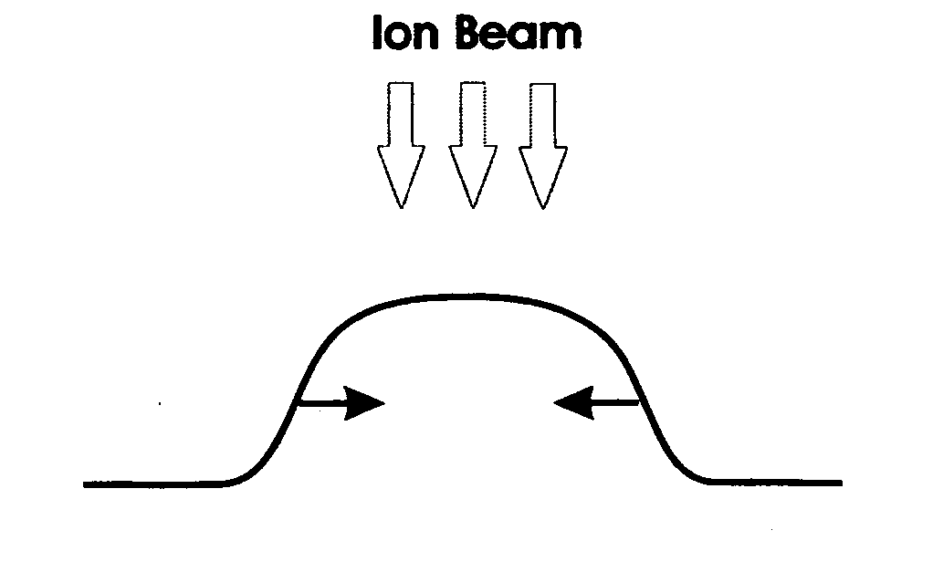
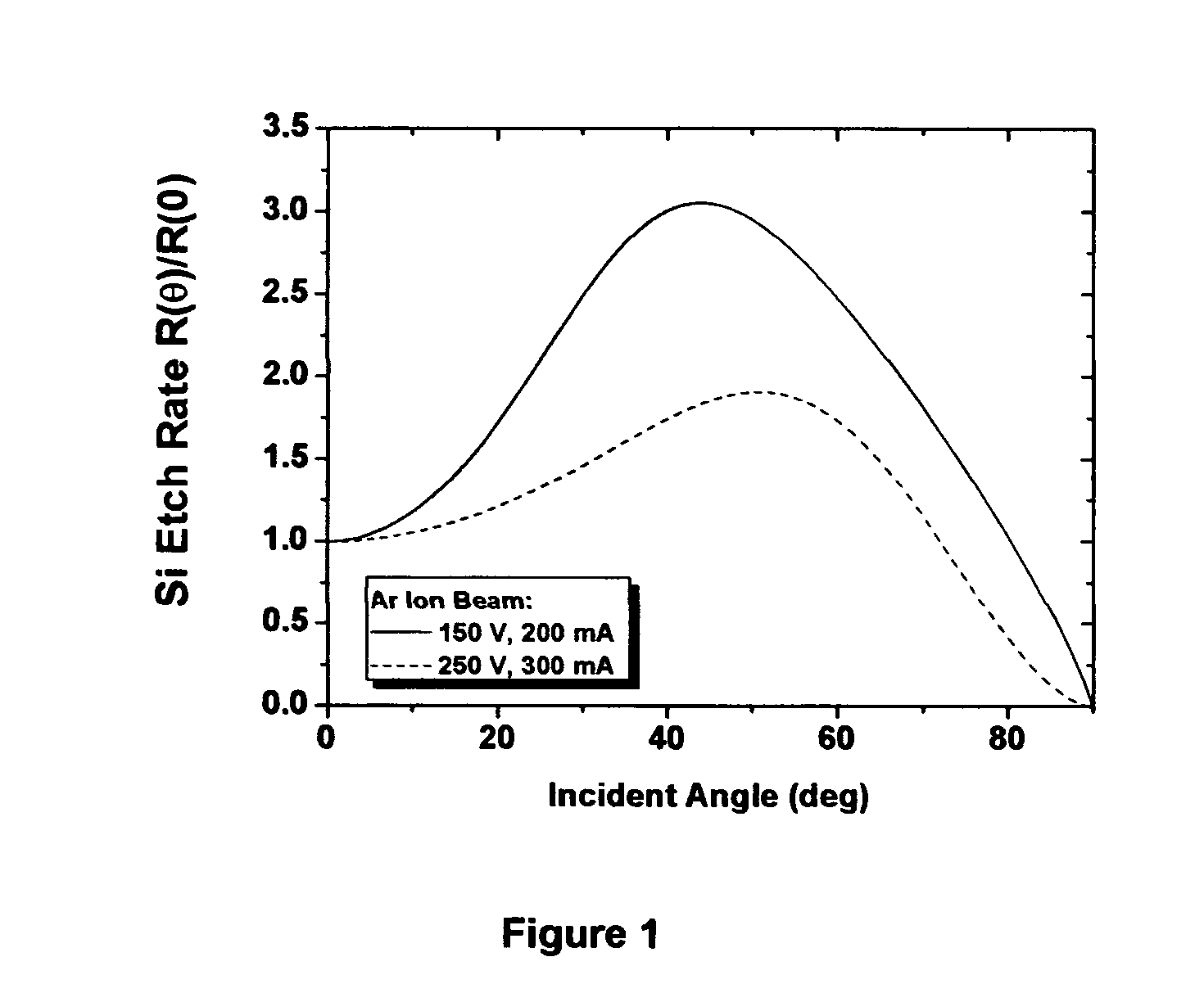
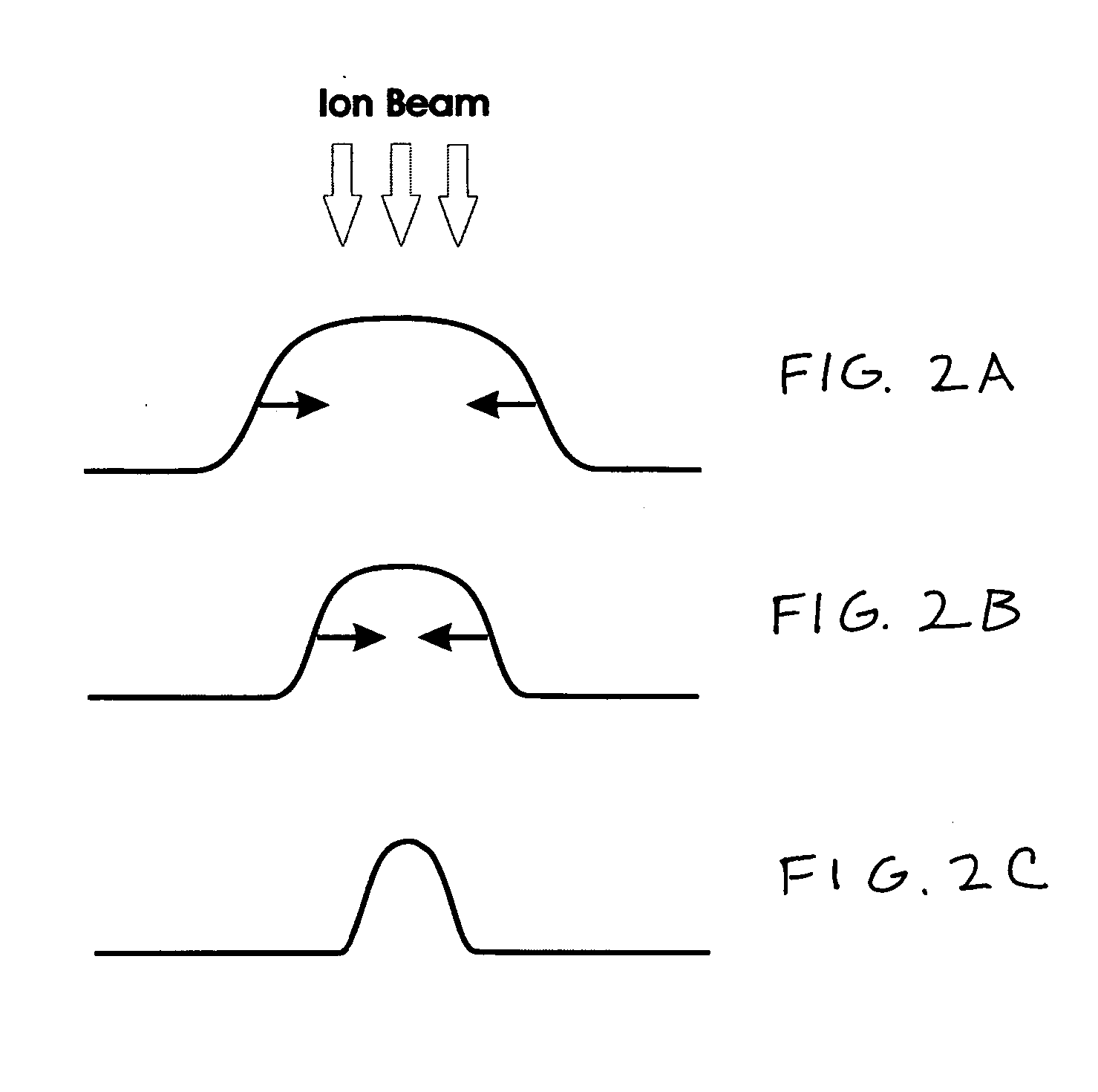
[0029] An embodiment of the invention includes a method for planarizing pits and scratches on substrates, especially on EUVL mask substrates. Another embodiment further includes planarizing particles on a substrate. The process includes depositing a film on a substrate and etching the film at an angle of incidence away from normal incidence. In practice it is useful to repeat the deposition and etch steps in a periodic sequence to enhance the planarization process and suppress surface roughening. The key planarization mechanism in this process is shadowing, as illustrated in FIG. 4. Due to shadowing, the etch rate at the bottom of the pit or scratch is essentially zero. The large difference between the etch rates at the surface of the film and the bottom of the defect causes the depth of the defect to rapidly decrease.

[0030] In order to test the pit planarization process, substrates with suitable pit defects were obtained. Samples with 70 nm deep and wide pit...


PUM

PropertyMeasurementUnit
Angleaaaaaaaaaa
Angleaaaaaaaaaa
Angleaaaaaaaaaa

Abstract

Ion-beam based deposition technique are provided for the planarization of pit and scratch defects in conjunction with particle defects. One application of this planarization technique is to mitigate the effects of pits and scratches and particles on reticles for extreme ultraviolet (EUV) lithography. In the planarization process, thin Si layers are successively deposited and etched away where the etching is directed at angles well away from normal incidence to the substrate to planarize pits and scratches without causing the particle defects to get too large; this is followed by a normal incidence etching process sequence designed primarily to planarize the particles but which will also planarize the pits and scratches to completion. The process also shows significant promise for planarizing substrate roughness.

Description

[0001] This application is a continuation-in-part of U.S. patent application Ser. No. 10 / 086,614, titled: “Ion-Assisted Deposition Techniques For The Planarization Of Topological Defects,” Filed Mar. 1, 2002, incorporated herein by reference.[0002] The United States Government has rights in this invention pursuant to Contract No. W-7405-ENG48 between the United States Department of Energy and the University of California for the operation of Lawrence Livermore National Laboratory.BACKGROUND OF THE INVENTION [0003] 1. Field of the Invention [0004] The present invention relates to the reduction of defects of extreme ultraviolet lithography mirrors, and more specifically, it relates to planarizing pits and scratches in the substrates of such mirrors and the ability to do so while simultaneously planarizing substrate particles. [0005] 2. Description of Related Art [0006] Reticle blanks for extreme ultraviolet lithography are fabricated by depositing reflective multilayer coatings such a...

Claims


Application Information

Patent Timeline
IPC IPC(8): C23C14/14C23C14/22C23C14/34C23C14/46C23C14/58G02B1/12G03F1/08G03F1/14G21K1/06
CPCB82Y10/00B82Y40/00C23C14/14C23C14/223C23C14/3442G21K2201/067C23C14/5833G02B1/12G03F1/08G03F1/24G21K1/062C23C14/46
Inventor MIRKARIMI, PAUL B.BAKER, SHERRY L.STEARNS, DANIEL G.SPILLER, EBERHARD A.
Owner MIRKARIMI PAUL B
Why Eureka
Try Eureka