

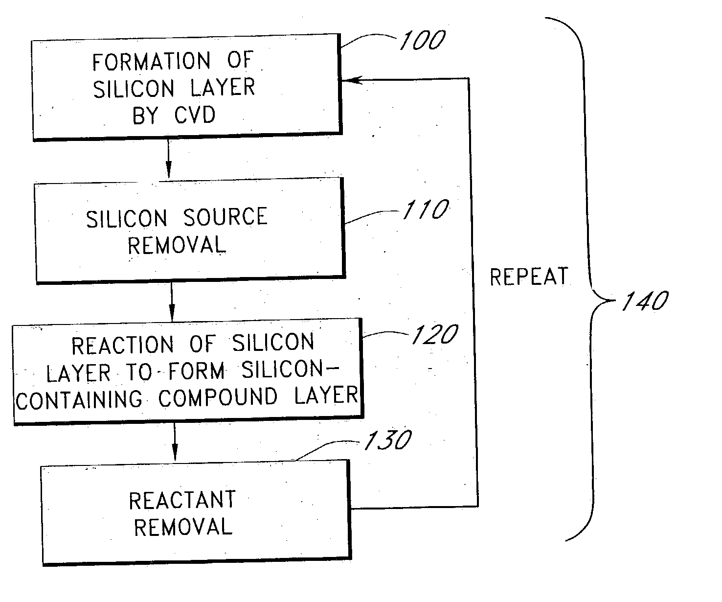
Method to form ultra high quality silicon-containing compound layers
a compound layer, ultra high-quality technology, applied in the direction of chemical vapor deposition coating, semiconductor/solid-state device details, coatings, etc., can solve the problems of cvd reducing throughput, ald being relatively inefficient in speed, and cvd being difficult to achiev
- Summary
- Abstract
- Description
- Claims
- Application Information
AI Technical Summary
Problems solved by technology
Method used
Image

Examples
example
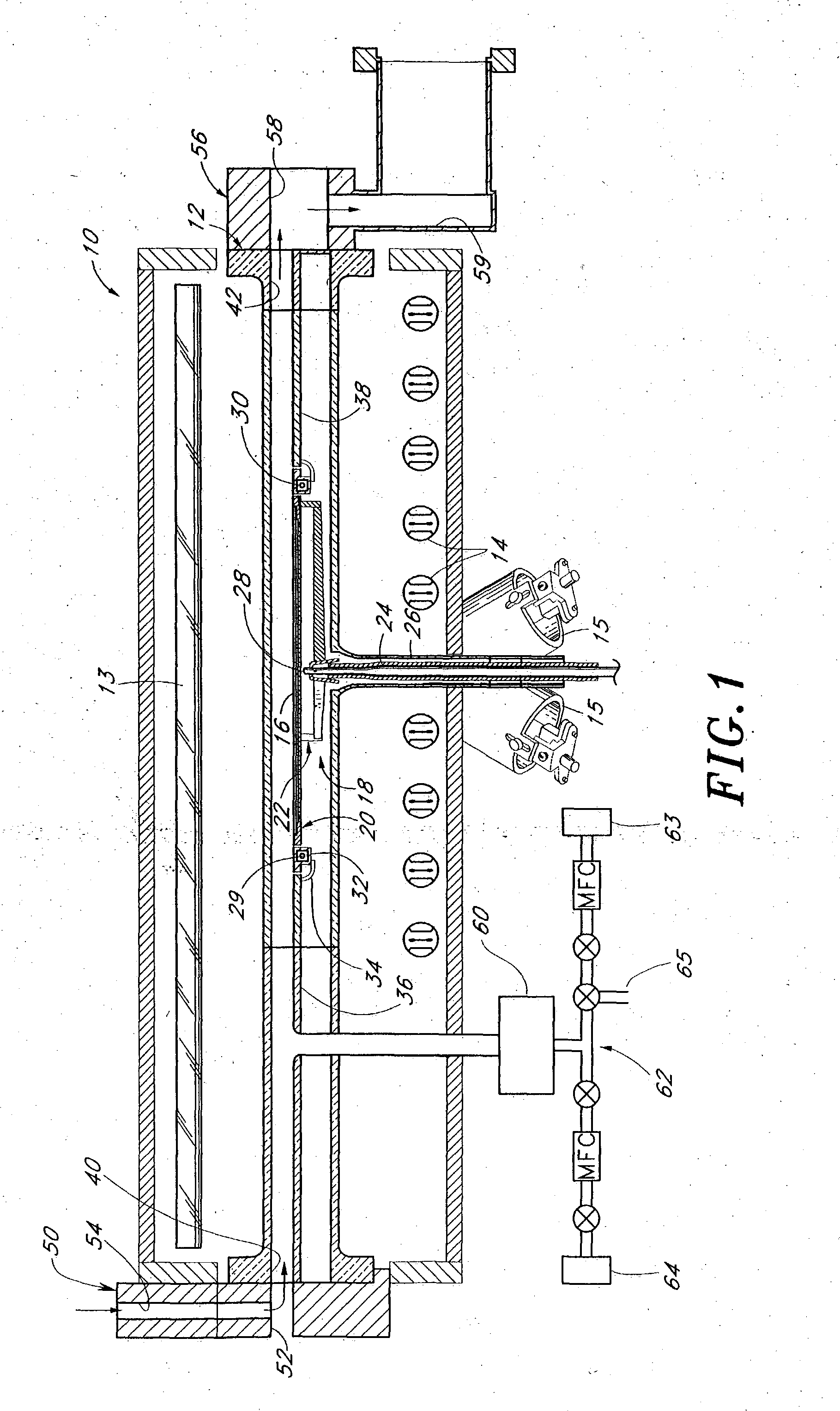
[0151] An exemplary method of forming the illustrated gate structure will now be described in detail:
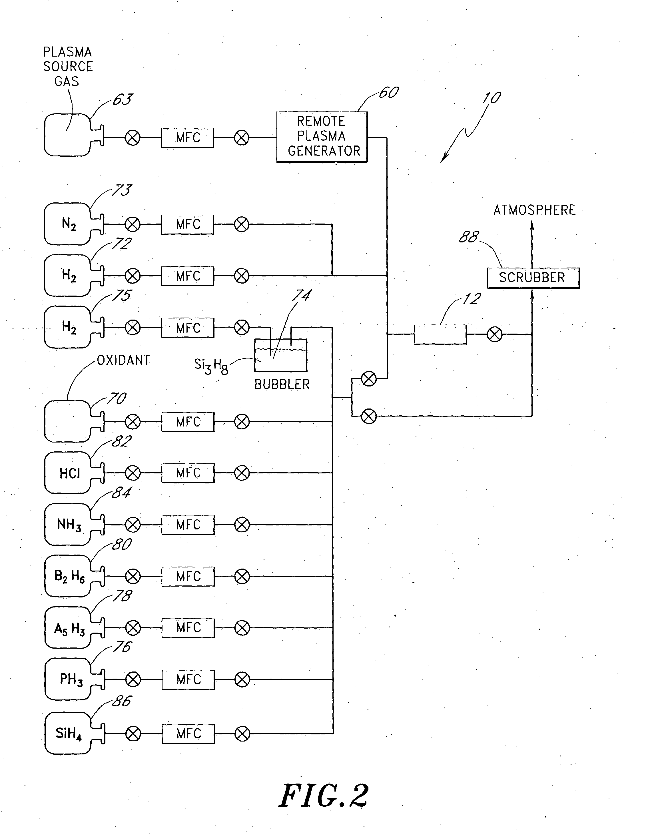
[0152] A silicon nitride layer was formed in a single substrate Epsilon™ reactor from ASM America, Inc. of Phoenix, Ariz. A wafer was loaded into the reaction chamber and prepared for trisilane deposition. Trisilane was flowed into the reaction chamber for 6 seconds at 63 sccm. The reaction chamber was purged for 10 seconds with nitrogen gas. Atomic nitrogen was generated by flowing nitrogen gas into a microwave radical generator (MRG) at 6 slm and flowed into the reaction chamber for 145 seconds. The reaction chamber was then purged with nitrogen gas for 10 seconds. About 5 Å of silicon nitride was deposited per cycle and eight cycles were performed to form a silicon nitride layer of about 40 Å in thickness. Each step of each cycle was performed isothermally at 650° C. and isobarically at 3 Torr.
PUM
| Property | Measurement | Unit |
|---|---|---|
| temperature | aaaaa | aaaaa |
| temperature | aaaaa | aaaaa |
| temperature | aaaaa | aaaaa |
Abstract
Description
Claims
Application Information