Electrolytic plating method and device for a wiring board

Inactive Publication Date: 2005-06-09
TOYOTA IND CORP
View PDF6 Cites 9 Cited by
  • Summary
  • Abstract
  • Description
  • Claims
  • Application Information

AI Technical Summary

Benefits of technology

[0016] With the above described configuration, the deposit speed of metal plating on the surface of a printed-circuit board and that of metal plating within a m

Problems solved by technology

With this method, however, it is difficult to further form one microvia hole on another, and to securely connect the holes in an electric manner.
Therefore, a land cannot be arranged on a microvia hole after microvia holes are stacked.
Due to such a restriction on a pattern design, the whole of a pattern design cannot be made with an automatic wiring tool, and part of the design must be made manually.
As a result, the time period required to design a printed-circuit b

Method used


Image

  • Electrolytic plating method and device for a wiring board
  • Electrolytic plating method and device for a wiring board
  • Electrolytic plating method and device for a wiring board

Examples


Embodiment Construction

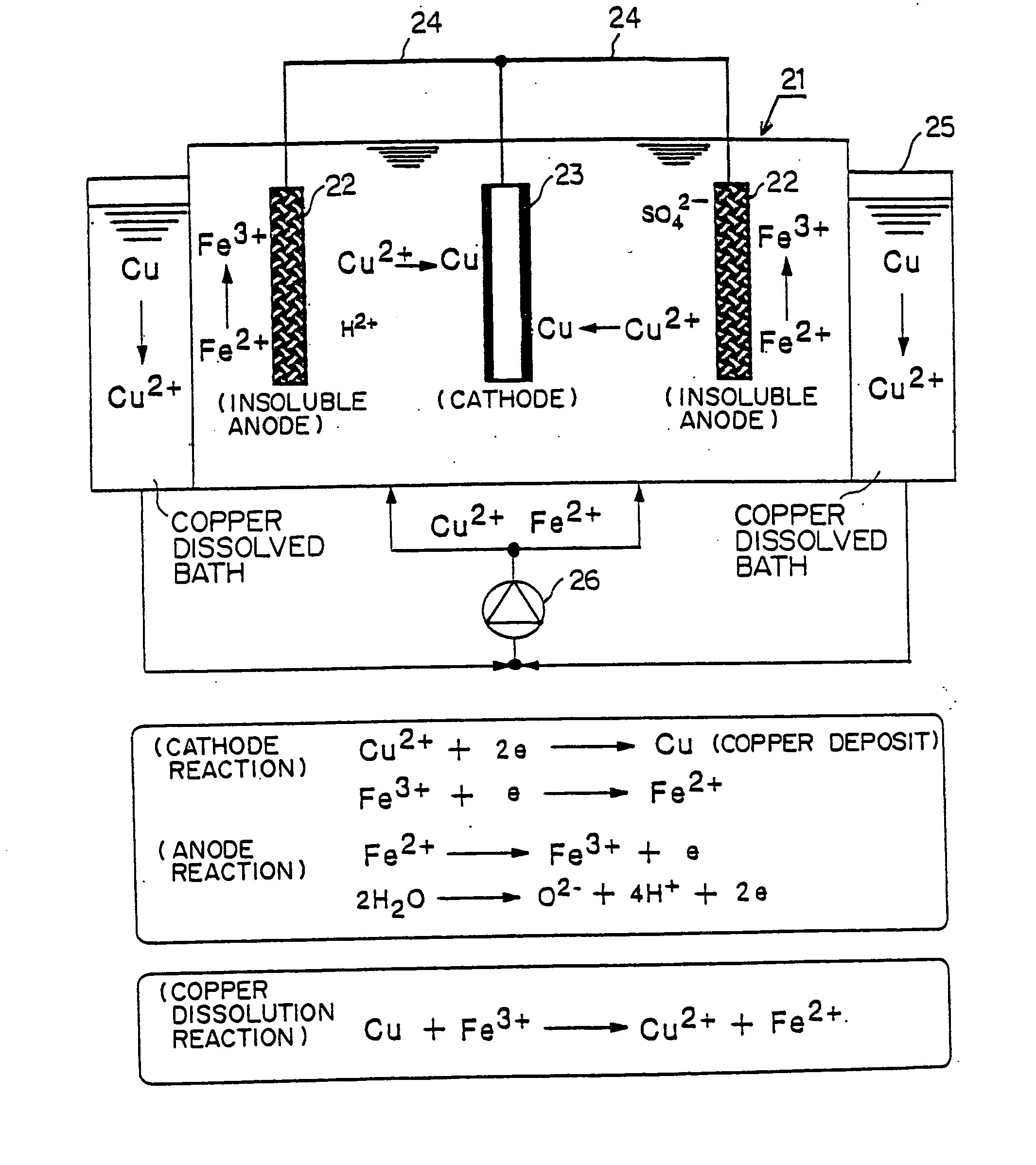
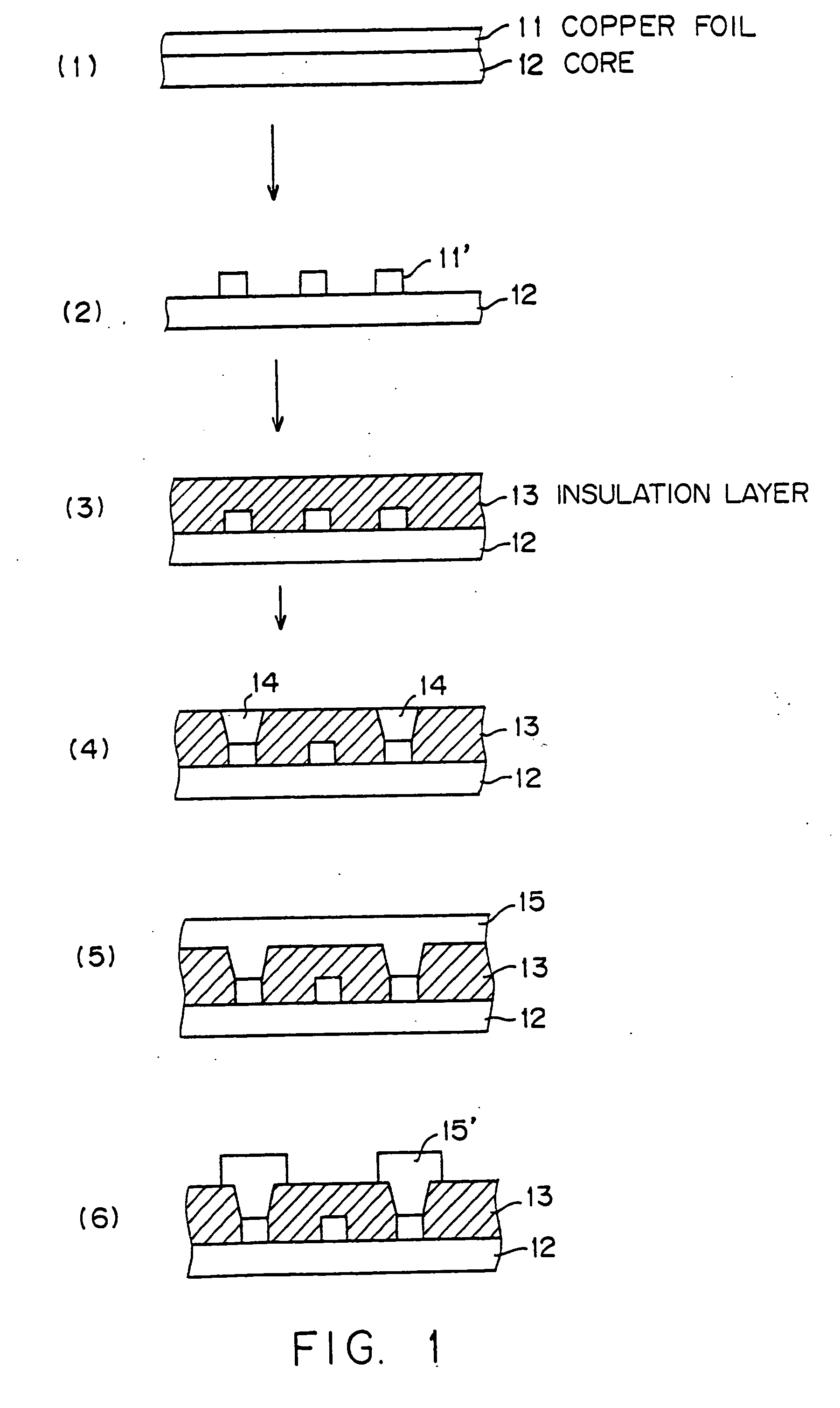
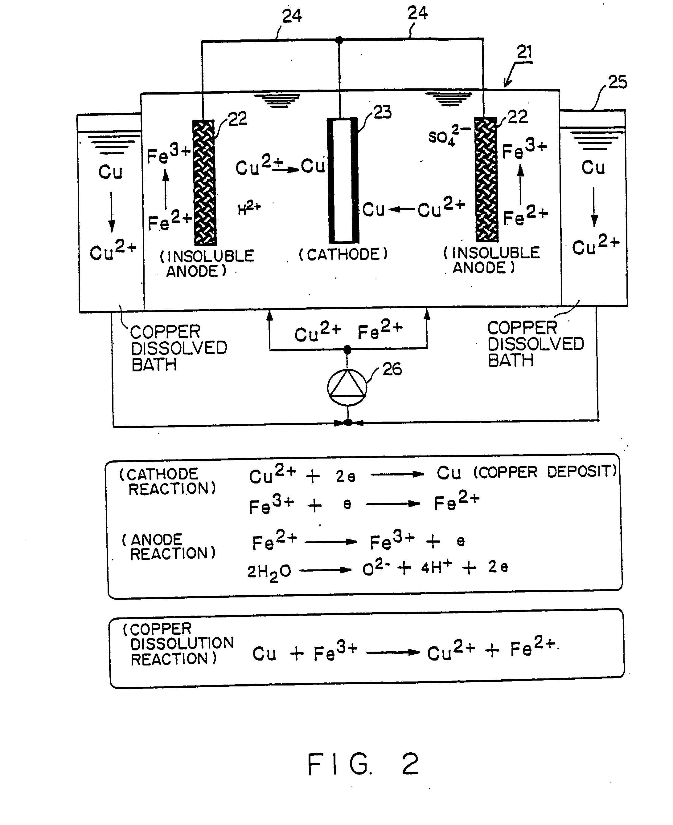
[0025] Hereinafter, a preferred embodiment according to the present invention will be described by referencing drawings. First of all, the manufacturing process of a multi-layer printed-circuit board is explained by referencing FIG. 1.

[0026] A wiring pattern (wiring layer) 11′ is formed by etching a copper foil (conductor layer) stacked onto a core resin 12 such as glass epoxy, etc. (process steps (1) and (2) in FIG. 1). Next, an insulation layer 13 is formed on the wiring pattern (process step (3) in FIG. 1). Holes are drilled in the insulation layer 13 with laser, etc., so that microvia holes 14 are formed (process step (4) in FIG. 1). Next, a copper plated layer 15 is formed with electrolytic plating, etc. to fill up the microvia holes (process step (5) in FIG. 1). In the plating process step (5) in FIG. 1, after a thin conductor layer is formed with chemical plating, etc. on the wiring pattern 11′ at the bottom of the insulation layer 13 and the microvia holes 14, the microvia ...


PUM

PropertyMeasurementUnit
Densityaaaaaaaaaa
Thicknessaaaaaaaaaa
Flow rateaaaaaaaaaa

Abstract

A plating bath which accommodates an insoluble node and a printed-circuit board, and a copper dissolved bath which supplies copper ions are arranged. The insoluble anode Is arranged as opposed to the printed-circuit board being a cathode, and a forward/reverse current is applied between both of the electrodes. Iron ions are added to a plating solution.

Description

BACKGROUND OF THE INVENTION [0001] 1. Field of the Invention [0002] The present invention relates to an electrolytic plating method and device filling up a microvia hole formed on a wiring board with metal plating. [0003] 2. Description of the Related Art [0004] For electric appliances such as a cellular phone, a video camera, a notebook computer, etc., it is demanded to mount high-density components. As an implementation of high-density mounting, a buildup board on which a wiring layer and an insulation layer are sequentially formed, a printed-circuit board of an all-layer microvia type to which wiring boards on which microvias are formed are attached with heat and pressure, etc. are proposed. [0005] For a conventional buildup board, micro holes (microvia holes) are formed on an insulation layer, and the inner side and the bottom of the holes are metal-plated, so that wiring layers above and below the insulation layer are electrically connected. [0006] With this method, however, it...

Claims


Application Information

Patent Timeline
IPC IPC(8): C25D5/18C25D3/38C25D7/00C25D21/14H05K3/18H05K3/42H05K3/46
CPCC25D5/18C25D21/14Y10S204/09H05K2201/09563H05K2203/1492H05K3/423C25D5/611H05K3/42
Inventor INOUE, TOSHIKIKUMAGAI, KYOKO
Owner TOYOTA IND CORP
Why Eureka
Try Eureka