Chip and wafer integration process using vertical connections

a vertical connection and integrated circuit technology, applied in the direction of transistors, solid-state devices, basic electric elements, etc., can solve the problems of reducing manufacturing yield, increasing chip size and manufacturing process complexity, and developing larger and more complex chips, and achieve high through-via density, high fidelity, and high chip placement accuracy

Inactive Publication Date: 2005-06-09
GLOBALFOUNDRIES U S INC
View PDF48 Cites 34 Cited by
  • Summary
  • Abstract
  • Description
  • Claims
  • Application Information

AI Technical Summary

Benefits of technology

[0011] The plate may be a temporary handling plate to facilitate thinning of the substrate. If the plate is transparent to ablating radiation, it may be conveniently removed by ablating an interface between the layer and the plate.
[0014] The present invention offers a significant advantage in that the through-via is formed in the substrate without an expensive deep-via etching process. Via dimensions may be maintained with very high fidelity, which in turn permits a high density of through-vias. Furthermore, the use of vertical stud / via interconnections allows for highly accurate chip placement in the third dimension, similar to the highly accurate lateral chip placement described above.

Problems solved by technology

The need for greater functionality and performance in semiconductor devices has resulted in the development of larger and more complex chips.
In addition, it is often desirable to include several different functions on a single chip to obtain a “system on a chip,” which generally results in both an increased chip size and a more complicated manufacturing process.
These factors both tend to depress manufacturing yield.
It is estimated that many such complex chips, with areas greater than 400 mm2, will generally have very poor manufacturing yield (perhaps under 10%).
The overall size of the SOC therefore limits the space available for wirebonding to make the external connections.

Method used


Image

  • Chip and wafer integration process using vertical connections
  • Chip and wafer integration process using vertical connections
  • Chip and wafer integration process using vertical connections

Examples


Embodiment Construction

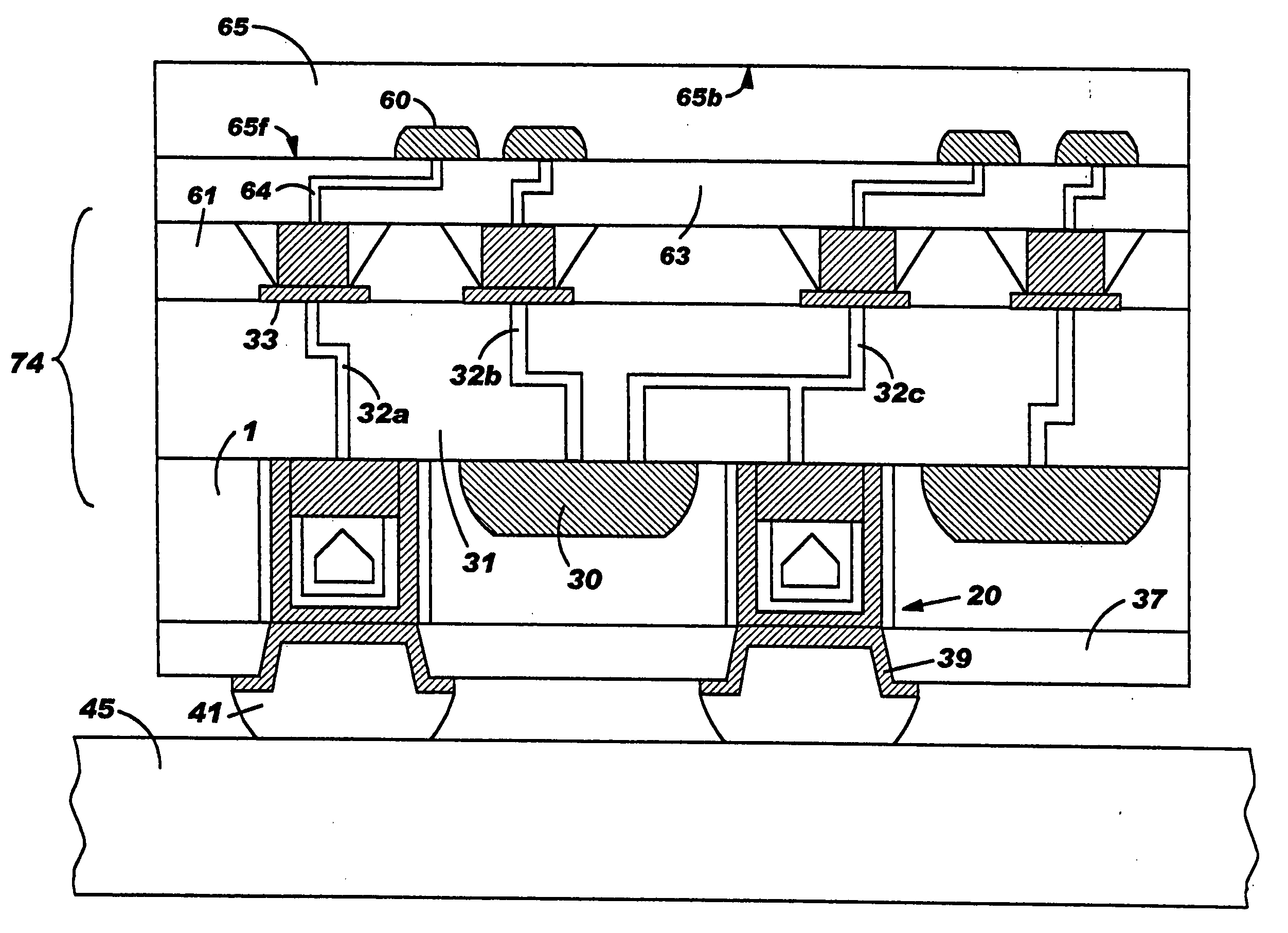
[0021] In accordance with the present invention, a semiconductor device is fabricated which includes vertical electrical connections through a chip. These vertical connections are formed by constructing metallized through-vias in the chip, without the need for expensive deep via etching.

[0022] In the embodiments discussed below, two different types of chips are vertically connected. Specifically, in the examples shown, a DRAM chip (or silicon DRAM device wafer) is vertically connected to a plurality of PE chips (or a silicon PE device wafer). It will be appreciated that these types of chips are discussed for purposes of illustration only, and that the present invention may be practiced with a wide variety of chips and wafer types.

Formation of Metallized vias

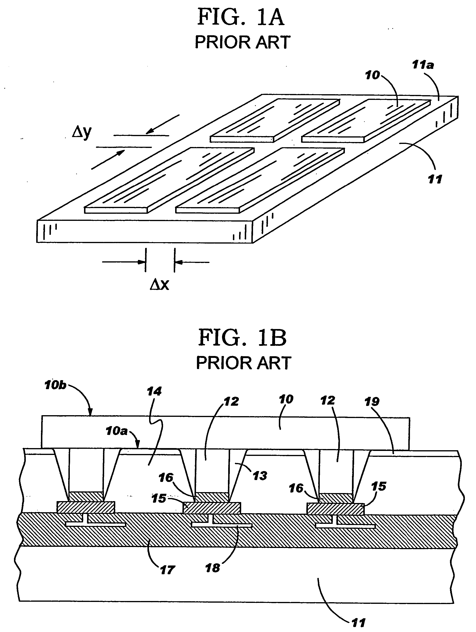
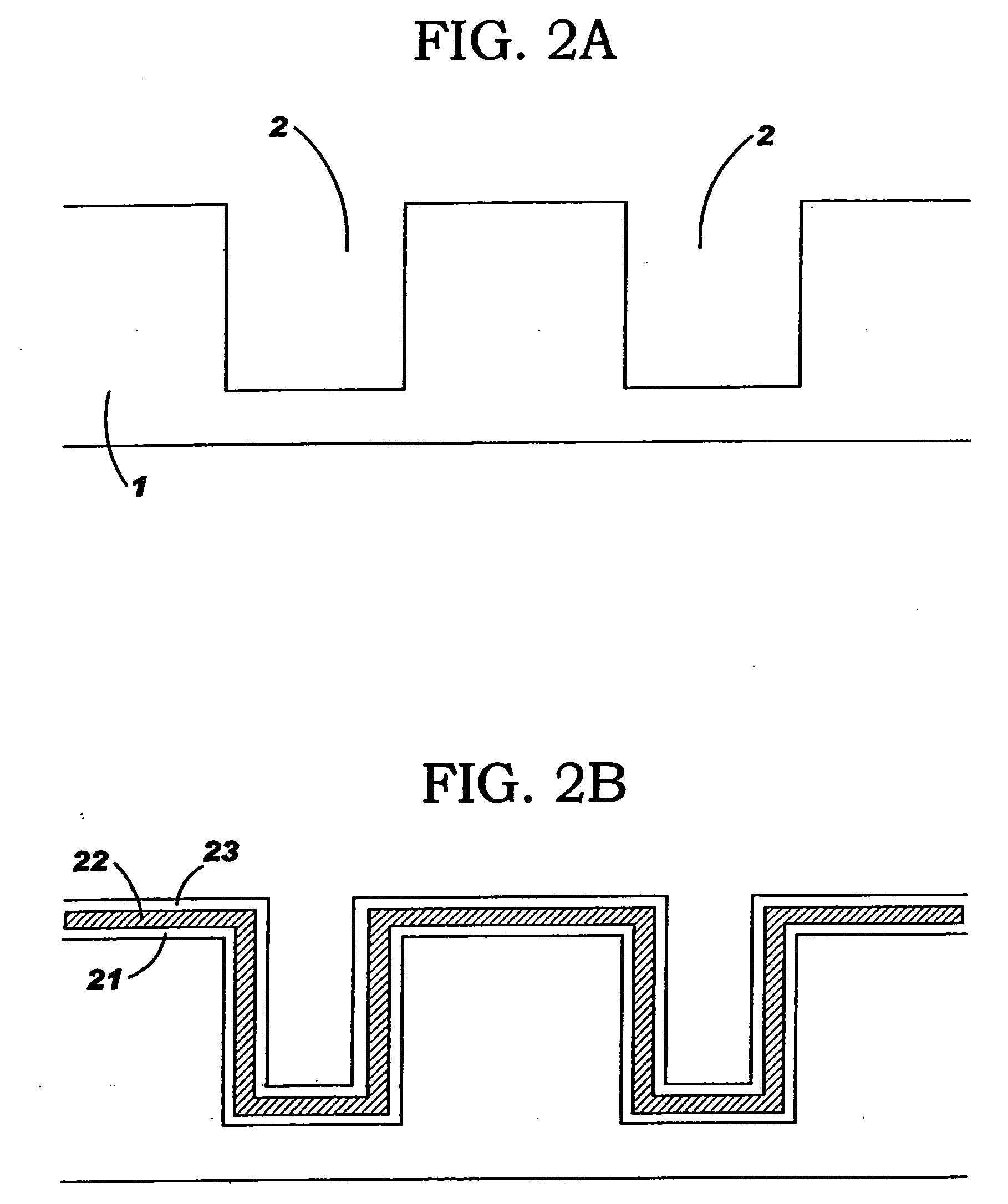
[0023] A metallized through-via in a semiconductor substrate, such as a silicon wafer, may be formed by depositing metal in a trench and thinning the wafer to open the bottom of the trench, as detailed below.

[0024] In a sili...


PUM


Abstract

A process is described for semiconductor device integration at chip level or wafer level, in which vertical connections are formed through a substrate. A metallized feature is formed in the top surface of a substrate, and a handling plate is attached to the substrate. The substrate is then thinned at the bottom surface thereof to expose the bottom of the feature, to form a conducting through-via. The substrate may comprise a chip having a device (e.g. DRAM) fabricated therein. The process therefore permits vertical integration with a second chip (e.g. a PE chip). The plate may be a wafer attached to the substrate using a vertical stud / via interconnection. The substrate and plate may each have devices fabricated therein, so that the process provides vertical wafer-level integration of the devices.

Description

FIELD OF THE INVENTION [0001] This invention relates to the manufacture of integrated circuit devices. More particularly, this application relates to a process for chip-level and wafer-level integration in which vertical interconnections are formed. BACKGROUND OF THE INVENTION [0002] The need for greater functionality and performance in semiconductor devices has resulted in the development of larger and more complex chips. In addition, it is often desirable to include several different functions on a single chip to obtain a “system on a chip,” which generally results in both an increased chip size and a more complicated manufacturing process. These factors both tend to depress manufacturing yield. It is estimated that many such complex chips, with areas greater than 400 mm2, will generally have very poor manufacturing yield (perhaps under 10%). [0003] One method of maintaining acceptable yields is to manufacture smaller chips, and then to interconnect those chips using lateral and v...

Claims


Application Information

Patent Timeline
Patent Type & Authority Applications(United States)
IPC IPC(8): H01L21/68H01L21/768H01L23/48H01L23/485H01L23/525H01L23/12H01L25/065H01L25/07H01L25/18
CPCH01L21/6835H01L21/76877H01L24/13H01L21/76898H01L23/481H01L23/525H01L24/10H01L25/0652H01L2224/0401H01L2224/13099H01L2224/16H01L2924/01004H01L2924/01022H01L2924/01027H01L2924/01029H01L2924/01033H01L2924/01039H01L2924/01057H01L2924/01061H01L2924/01074H01L2924/01078H01L2924/01079H01L2924/10329H01L2924/14H01L2924/01006H01L2924/014H01L24/81H01L2924/00H01L2224/03002H01L2224/0557H01L2224/06181H01L2224/16145H01L2224/17181H01L2224/81005H01L2224/94H01L2224/05572H01L2924/15787H01L2924/12042H01L2224/13H01L2224/05155H01L2224/05166H01L2224/05184H01L2224/05644H01L24/03H01L24/05H01L24/11H01L2224/11H01L2224/03H01L2924/00014H01L2924/013H01L21/768
Inventor POGGE, H. BERNHARDYU, ROYPRASAD, CHANDRIKANARAYAN, CHANDRASEKHAR
Owner GLOBALFOUNDRIES U S INC
Why Eureka
Try Eureka