Structure of an electromagnetic shield layer for a plasma display panel and method for manufacturing the same

a technology of electromagnetic shield layer and plasma display panel, which is applied in the direction of solid-state diffusion coating, superimposed coating process, transportation and packaging, etc., can solve the problems of reducing the efficiency of electromagnetic shielding, reducing the transparency of the substrate, and gluing, so as to avoid the influence of light reflection by the environment, the effect of excellent optical characteristics and adhesion qualities

Inactive Publication Date: 2007-06-07
NAT CHUNG SHAN INST SCI & TECH
View PDF3 Cites 18 Cited by
  • Summary
  • Abstract
  • Description
  • Claims
  • Application Information

AI Technical Summary

Benefits of technology

[0007] According to the present invention, metal layers are built inside plastic substrates. Thus, the problem of producing bubbles and voids when gluing can be prevented. In addition, according to the present invention, because the metal layers are recessed in the structure, the glue for assembly can be coated thinly, and is advantageous for thinning the whole structure as well as for the penetrating light. Because the conduction layer is a black oxidation layer itself, and because the metal layers are built inside the plastic substrates, it is only necessary to carry out black oxidation process to the surface of the metal layer then double-side black oxidation is generated. Thus, the influence of light reflection by environments can be avoided effectively. Consequently, optical characteristics and adhesion qualities are both excellent. Thereby, the product according to the present invention is far superior to the product according to the prior art both in quality and in cost.
[0008] The feature of the present invention is to use hot embossing, coating, and electroplating technologies to manufacture a metal layer built inside a substrate of plastic material and having electromagnetic-wave shielding effect, and thus to provide excellent optical transparency characteristics as well as electromagnetic-wave shielding capabilities. The geometric pattern of the metal layer of the electromagnetic shield layer comprises 50 -micrometer or narrower linewidths, and 150 -micrometer or wider line pitches, such that the aspect ratios (the ratios of linewidth to line pitch) are above 75%. In addition, the thickness of the metal layer is between 1 micrometer and 15 micrometers. The materials of the metal layer are composed of copper, nickel, copper alloy or nickel alloy. Besides, the advantage of being built inside the plastic materials is used to generate double-side black oxidation so that the influence of light reflection by environments can be avoided.
[0009] The master mold for hot embossing in the manufacturing method of the electromagnetic shield layer according to the present invention can be made using lithography and electroplating, in which nickel-cobalt master molds can be manufactured with linewidths between 6 and 50 micrometers and line pitches between 150 and 500 micrometers, or can be made using laser machining on metal materials. In general, the mater molds can be used for tens of thousand times. In addition, molds are so easy to fabricate that subsequent requests of producing geometric patterns with different or identical depth can be satisfied. A substrate is hot embossed in a hot embossing machine. The substrate includes polymethyl methacrylate (PMMA), polycarbonate (PC), polyethylene terephthalate (PET), polyethyl (PE), methylstyrene (MS), and triacetate cellulose (TAC). With operating temperatures of hot embossing between 100 and 200° C. and pressures between 1000 and 4000 N, a plurality of substrates with trench widths between 6 and 50 micrometers, trench pitches between 150 and 500 micrometers, and depths between 1 and 15 micrometers can be manufactured smoothly. Metal glue is coated to trenches with a scraper, and are heated to 70˜150° C. and dried off to form a conduction layer. The coated conduction layer is formed by metal powder and glue mixed uniformly, wherein the metal powder includes silver, copper, nickel, gold, tin, platinum, palladium, iridium, cobalt, zinc, and

Problems solved by technology

However, the manufacturing cost of the sputtering method is high, and the transparency of the substrate reduces as the thickness of the sputtered layer increases.
One the other hand, if the thickness of the sputtered layer is reduced, the efficiency of electromagnetic shielding is relatively worse.
Thereby, transparency is the main issue of the method.
Owing to limitations of printing lines with precision, it is not possible to manufacture circuits with linewidth below 40 micrometers, which results in wider linewidths and consequently affects the overall transparency.
However, the investment cost of exposure equipments is costly if the electromagnetic shield layer is produced by lithography.
Moreover, there are many process challenges to be conquered.
Copper is prone to slight rolling-up due to different coefficients of thermal expansion with PE

Method used


Image

  • Structure of an electromagnetic shield layer for a plasma display panel and method for manufacturing the same
  • Structure of an electromagnetic shield layer for a plasma display panel and method for manufacturing the same
  • Structure of an electromagnetic shield layer for a plasma display panel and method for manufacturing the same

Examples


embodiment 1

Coated with Silver Glue Products

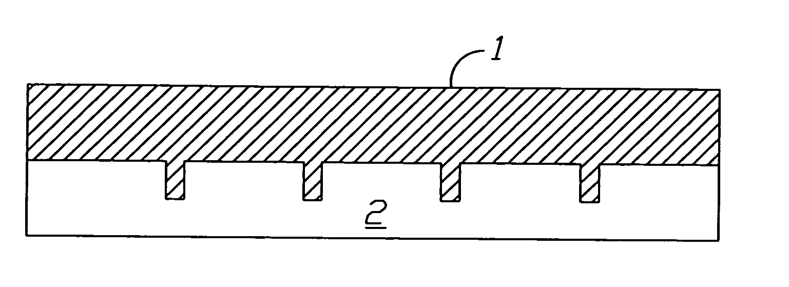
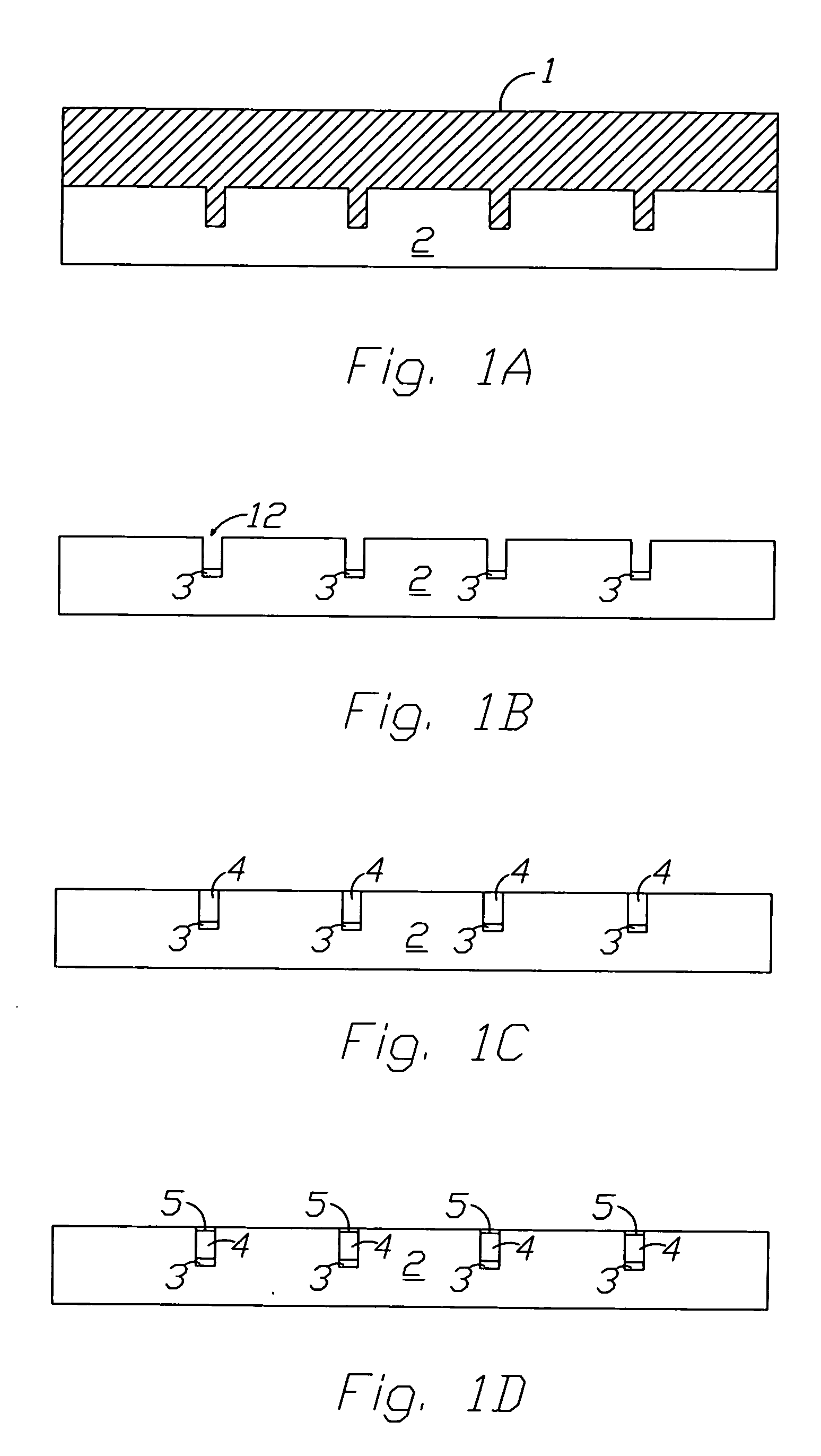
[0013] On a PMMA plastic material, meshed trenches with linewidth of 12 micrometers and line pitch of 290 micrometers using hot embossing method are formed, and a layer of silver glue in the meshed trenches is coated. The electromagnetic-wave shielding effect thereof is as follows. The shielding efficiency for electric field frequencies of 0˜500 MHz is between 21 and 50 dB, and is averaged to 27 dB; the shielding efficiency for electric field frequencies of 500-1000 MHz is between 15 and 21 dB, and is averaged to 18 dB. The shielding efficiency for magnetic field frequencies of 0˜600 MH is between 3 and 10 dB, and is averaged to 6 dB; the shielding efficiency for magnetic field frequencies of 600˜1000 MHz is between 10 and 20 dB, and is averaged to 15 dB.

embodiment 2

Electroplated with 2-Micrometer Copper

[0014] On a PMMA plastic material, meshed trenches with linewidth of 12 micrometers and line pitch of 290 micrometers using hot embossing method are formed, and a layer of silver glue in the meshed trenches is coated. In addition, increase the thickness of copper in the trenches to 2 micrometers using the copper electroplating technology. The electromagnetic-wave shielding effect thereof is as follows. The shielding efficiency for electric field frequencies of 0˜500 MHz is between 32 and 58 dB, and is averaged to 41 dB; the shielding efficiency for electric field frequencies of 500-1000 MHz is between 25 and 32 dB, and is averaged to 29 dB. The shielding efficiency for magnetic field frequencies of 0-600 MH is between 14 and 26 dB, and is averaged to 21 dB; the shielding efficiency for magnetic field frequencies of 600-1000MHz is between 26 and 40 dB, and is averaged to 36 dB.

embodiment 3

Electroplated with 2-Micrometer Nickel

[0015] On a PMMA plastic material, meshed trenches with linewidth of 12 micrometers and line pitch of 290 micrometers using hot embossing method are formed, and a layer of silver glue in the meshed trenches is coated. In addition, increase the thickness of nickel in the trenches to 2 micrometers using the nickel electroplating technology. The electromagnetic-wave shielding effect thereof is as follows. The shielding efficiency for electric field frequencies of 0˜500 MHz is between 22 and 57 dB, and is averaged to 32 dB; the shielding efficiency for electric field frequencies of 500˜1000 MHz is between 16 and 22 dB, and is averaged to 19 dB. The shielding efficiency for magnetic field frequencies of 0˜600 MH is between 7 and 21 dB, and is averaged to 13 dB; the shielding efficiency for magnetic field frequencies of 600˜1000 MHz is between 21 and 27 dB, and is averaged to 24 dB.


PUM

PropertyMeasurementUnit
Temperatureaaaaaaaaaa

Abstract

A structure of an electromagnetic shield layer for a plasma display panel and a method for manufacturing the same. The manufacturing method of the electromagnetic shield layer uses integrated technologies of hot embossing, coating, and electroplating. The structure according to the present invention is a metal layer with an electromagnetic-wave shielding effect and is built in a plastic material. The aspect ratios of the geometric patterns on the metal layer are above 75%.

Description

FIELD OF THE INVENTION [0001] The present invention relates generally to a structure of an electromagnetic shield layer and a method for manufacturing the same, and particularly to a structure of an electromagnetic shield layer for a plasma display panel and a method for manufacturing the same. The electromagnetic shield layer is adapted on the front surface of the display to shield electromagnetic-wave radiations. Thereby, the class B specification for home applications can be complied with, and impacts on human health can be avoided. BACKGROUND OF THE INVENTION [0002] With the advancements of technologies, the United States will start to switch to digital televisions. When the time comes, plasma display panels will become popular as consumers enjoy digital television programs. For examples, a plasma television uses the principles of a fluorescent light and a neon light to fill inert gas such as neon (Ne) and xenon (Xe) to a micro duct. The ultraviolet light generated by discharge ...

Claims


Application Information

Patent Timeline
IPC IPC(8): B32B3/00
CPCC23C8/02C23C28/023H01J9/205Y10T428/24612H05K9/0096C23C28/021C23C28/025H01J2211/446
Inventor TSO, CHING-YUSHY, HSIOU-JENGWU, HSIEN-MINGSHU, WEN-YUNGCHENG, JOSEPH
Owner NAT CHUNG SHAN INST SCI & TECH
Why Eureka
Try Eureka