Touch screen and manufacturing method thereof

A manufacturing method and touch screen technology, applied in the direction of instruments, electrical digital data processing, input/output process of data processing, etc., to achieve the effect of improving high adhesion

Inactive Publication Date: 2016-10-12
TRULY OPTO ELECTRONICS
View PDF8 Cites 19 Cited by
  • Summary
  • Abstract
  • Description
  • Claims
  • Application Information

AI Technical Summary

Problems solved by technology

However, at present, the touch screen made of nano-silver as the conductive film material needs to be improved in terms of high adhesion, thinning, and bending resistance, so as to meet the development needs of subsequent special-shaped, curved or flexible products.

Method used


Image

  • Touch screen and manufacturing method thereof
  • Touch screen and manufacturing method thereof

Examples


Embodiment 1

[0033] This embodiment provides a method for manufacturing a touch screen, which includes the following steps:

[0034] Step 1. Provide a TCTF integrating a dry film and a nano-silver conductive layer and a flexible substrate with a first patterned conductive film.

[0035] The conductive material of the first patterned conductive film is nano-silver particles and / or nano-silver wires, which are formed on the flexible substrate after etching. The flexible substrate can be an ultra-thin glass or plastic substrate. In this embodiment, it is preferably a polymer plastic substrate, and the thickness is preferably about 2-50 μm. The etching method may be yellow photoetching or laser etching.

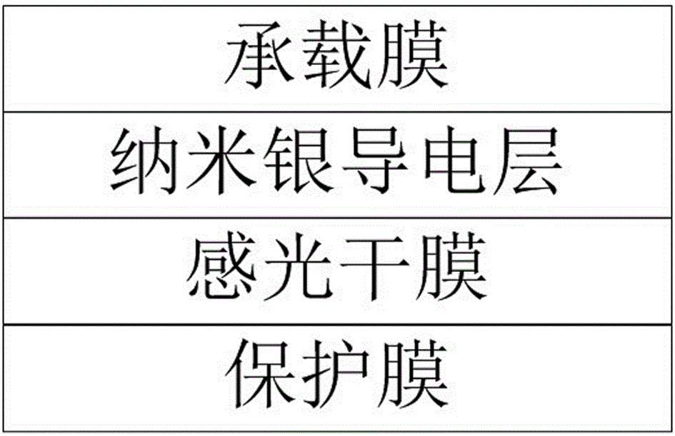
[0036] like figure 1 As shown, the TCTF includes a photosensitive dry film, a nano-silver conductive layer coated on the photosensitive dry film and cured, a carrier film positioned on the nano-silver conductive layer, and a film for protecting the photosensitive dry film. protective film...

Embodiment 2

[0046] The only difference between this embodiment and Embodiment 1 is that the manufacturing method of the flexible substrate includes the following steps:

[0047] Step A1, curing and forming a conductive film on the rigid substrate, the material for forming the conductive film is nano-silver wire and / or nano-silver particle.

[0048]After curing, the resistance of the conductive layer of the conductive film is preferably 50-80Ω / □, and the transmittance is >90%. The curing temperature of the conductive film is 120-160° C., and the curing time is 10-60 minutes. Preferably, the curing temperature is 150° C., and the curing time is 30 minutes.

[0049] The rigid substrate is a tempered or non-tempered substrate, preferably a glass substrate in the present invention.

[0050] Step A2, printing conductive silver paste on the frame of the conductive film.

[0051] Step A3, performing laser etching on the conductive film and the conductive silver paste at the same time to obtain ...

Embodiment 3

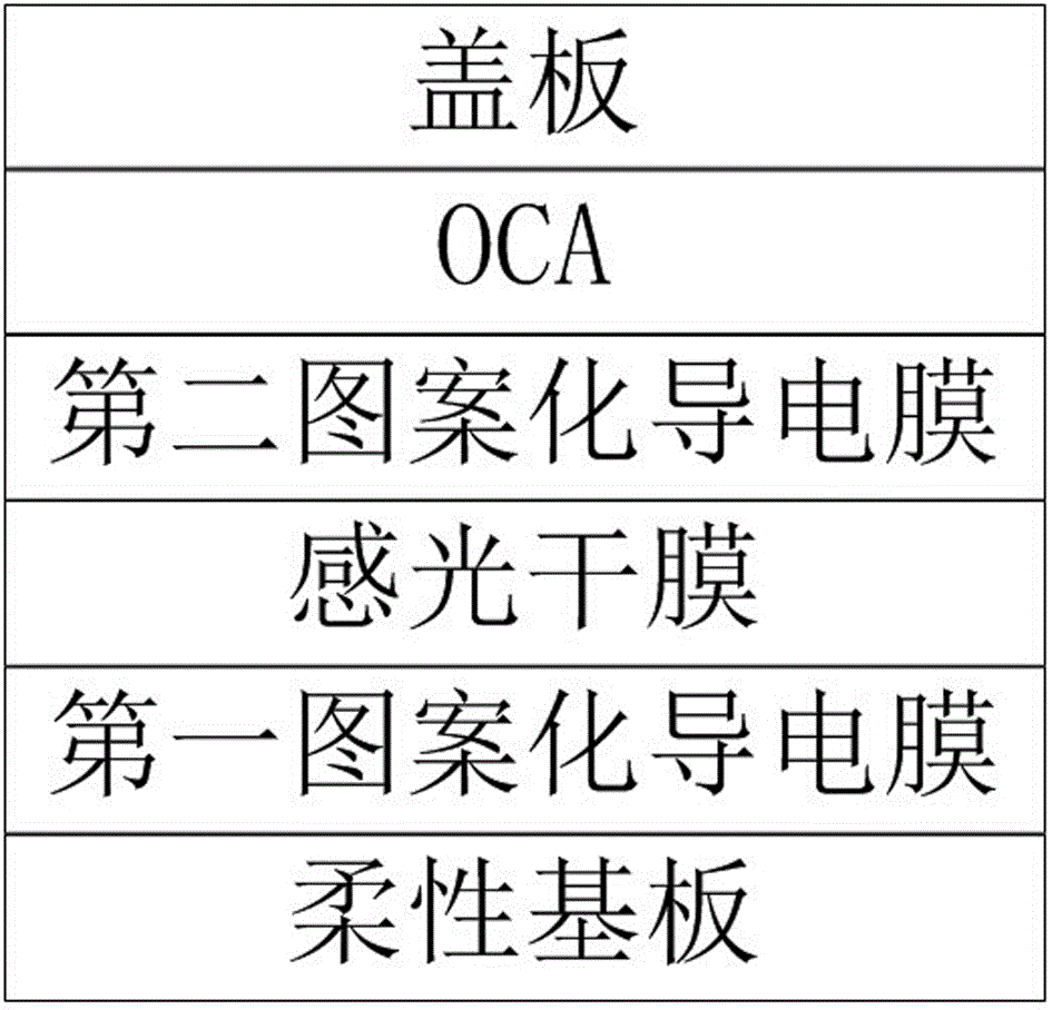
[0060] like figure 2 As shown, the present embodiment provides a touch screen, comprising: a flexible substrate having a first patterned conductive film, a TCTF integrating a dry film and a nano-silver conductive layer, the conductive surface of the flexible substrate faces the TCTF The non-conductive surface is relatively attached and bonded to the circuit board, and a second patterned conductive film is formed on the TCTF by exposure and development.

[0061] Further, the conductive material of the first patterned conductive film is nano-silver particles and / or nano-silver wires.

[0062] Further, the patterns of the first patterned conductive film and the second patterned conductive film are the same or different.

[0063] Further, the flexible substrate may be an ultra-thin glass or plastic substrate, and in this embodiment, it is preferably a polymer plastic substrate, and the thickness is preferably about 2-50 μm.

[0064] like figure 1 As shown, the TCTF includes a...


PUM


Abstract

The invention discloses a touch screen and a manufacturing method thereof. The manufacturing method comprises the following steps: providing TCTF and a flexible substrate, wherein the TCTF integrates a dry film and a nano-silver conducting layer, the flexible substrate comprises a first patterned conducting film, and the conducting materials of the first patterned conducting film comprise nano-silver particles and/or nano-silver wires; relatively laminating a conducting surface of the flexible substrate with a non-conducting surface of the TCTF; carrying out exposure development on a conducting surface of the TCTF, so as to form a second patterned conducting film. According to the manufacturing method, an ultrathin touch screen structure formed by the nano-silver flexible substrate and the TCTF integrating the dry film and the nano-silver conducting layer is selected, the conducting surface of the flexible substrate is laminated with the non-conducting surface of the TCTF, a patterned conducting layer is formed after the exposure development of the conducting surface of the TCTF, and then the cambered or flexible touch screen is manufactured; a high-adhesion, thinned and bending-resistant double-layer nano-silver touch screen is manufactured, and great possibility is provided for the development of subsequent irregular, cambered or flexible products.

Description

technical field [0001] The invention relates to the technical field of touch screens, in particular to a touch screen and a manufacturing method thereof. Background technique [0002] The touch screen is an input device that significantly improves the man-machine interface, and has the advantages of intuition, simplicity and speed. Touch screens have been widely used in many electronic products, such as mobile phones, PDAs, multimedia, public information inquiry systems, and the like. Taking the GFF structure capacitive touch screen as an example, its basic structure is the emission layer, OCA, reception layer, OCA and cover glass; the emission layer and the reception layer are both patterned transparent conductive films. The transparent conductive film of the traditional CTP (OGS / TOL and GFF, etc.) structure touch screen is made of ITO coating through laser etching, screen printing, yellow light etching and other methods. [0003] However, with the popularization of curve...

Claims


Application Information

Patent Timeline
Patent Type & Authority Applications(China)
IPC IPC(8): G06F3/042G06F3/041
CPCG06F3/0412G06F3/042G06F2203/04103
Inventor 刘欣邱泽银周伟杰李锋李志成李建华
Owner TRULY OPTO ELECTRONICS
Why Eureka
Try Eureka