Planar waveguide optical isolator in thin silicon-on-isolator (SOI) structure

Inactive Publication Date: 2005-06-09
CISCO TECH INC
View PDF16 Cites 110 Cited by
  • Summary
  • Abstract
  • Description
  • Claims
  • Application Information

AI Technical Summary

Benefits of technology

[0013] An advantage of the SOI-based, planar optical isolator of the present invention is that an additional, patterned polysilicon layer may be formed over certain portions of the waveguide structure and

Problems solved by technology

Without the isolator, unwanted optical signals (i.e., reflections) from the optical fiber would couple back into the DFB laser and adversely affect its transmitted optical spectrum.
The monolithic integration of a conventional Faraday isolator int

Method used


Image

  • Planar waveguide optical isolator in thin silicon-on-isolator (SOI) structure
  • Planar waveguide optical isolator in thin silicon-on-isolator (SOI) structure
  • Planar waveguide optical isolator in thin silicon-on-isolator (SOI) structure

Examples


Embodiment Construction

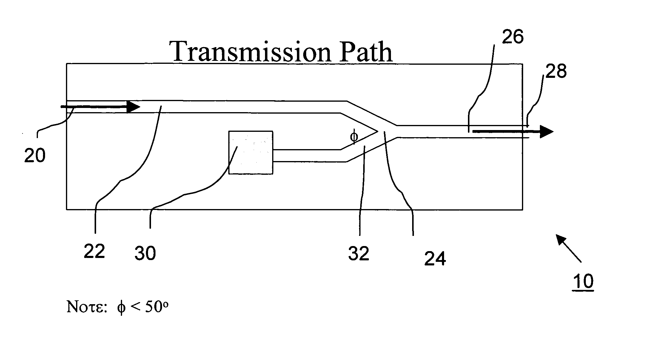
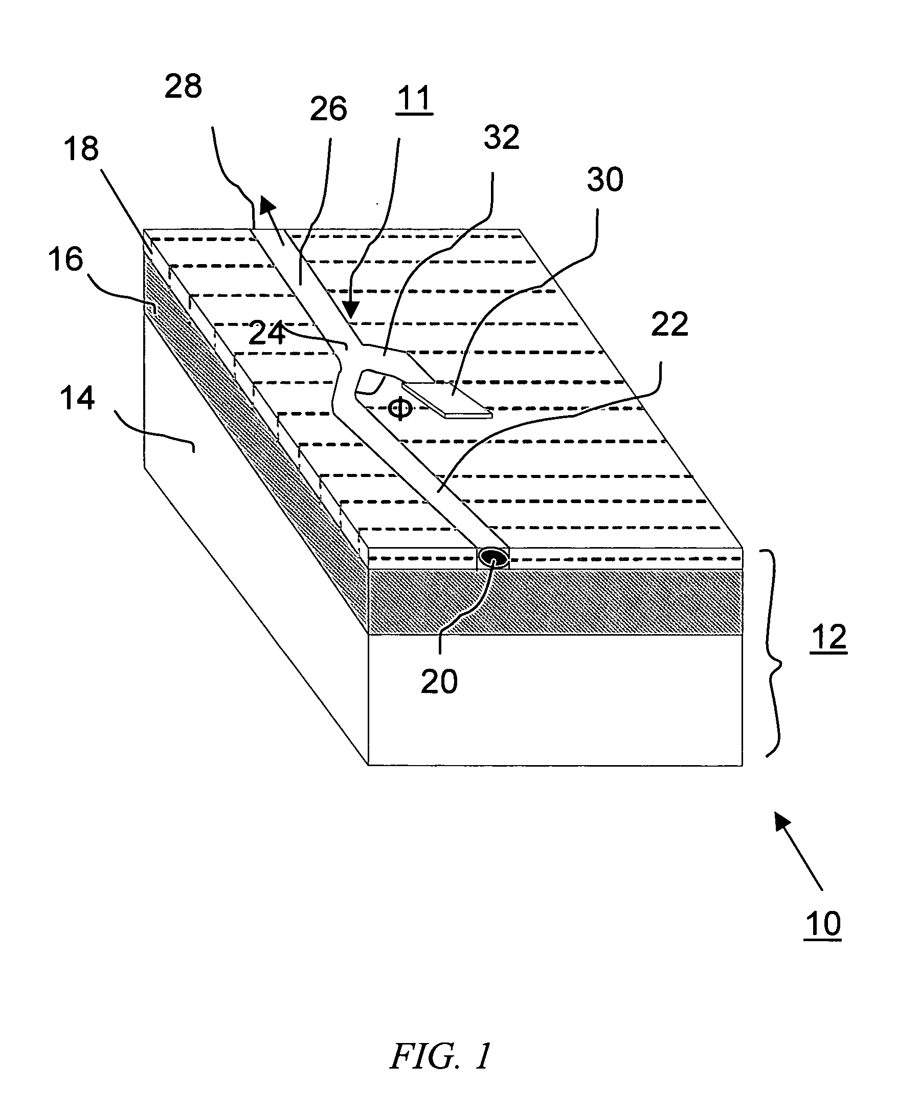
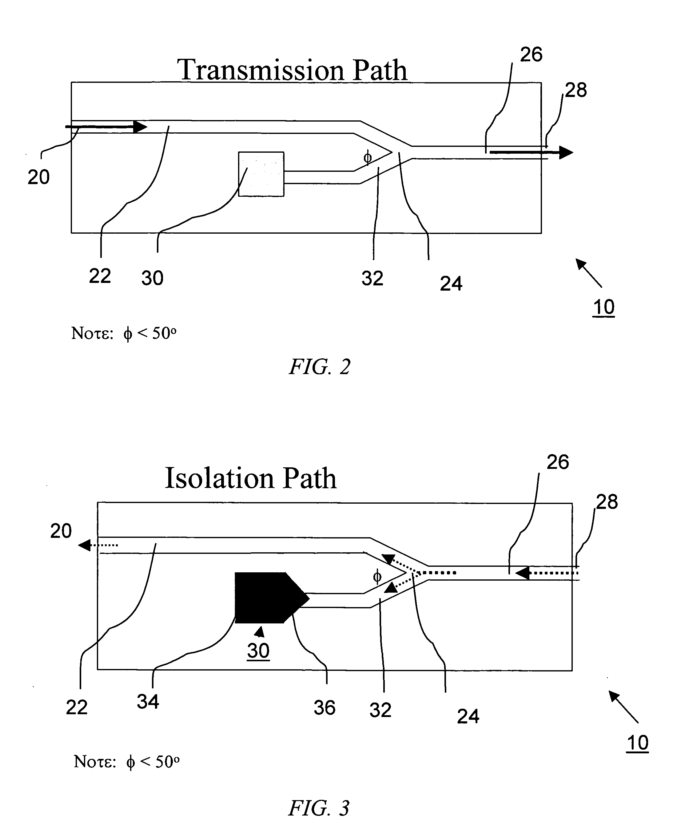
[0032]FIG. 1 contains an isometric view of an exemplary SOI-based planar optical isolator 10 formed in accordance with the present invention. Optical isolator 10 is formed within a silicon-on-insulator (SOI) structure 12 comprising a silicon substrate 14, an insulating dielectric layer 16 (usually comprising SiO2) and a surface single crystal silicon layer 18 (typically referred to in the art as the “SOI layer”). In most cases, SOI layer 18 will comprise a thickness of less than one micron. In some cases, the surface silicon layer may comprise a “strained” silicon layer, where the lattice structure of the silicon has been modified. Although not particularly illustrated in FIG. 1, or any of the following drawings, it is to be understood that in actual use, the associated opto-electronic components are formed within the same SOI structure 12, thus forming an efficient, monolithic optical system arrangement.

[0033] In accordance with the present invention, optical isolator 10 includes ...


PUM


Abstract

A planar optical isolator is formed within the silicon surface layer of an SOI structure. A forward-directed signal is applied to an input waveguiding section of the isolator and thereafter propagates through a non-reciprocal waveguide coupling region into an output waveguide section. A rearward-directed signal enters via the output waveguide section and is thereafter coupled into the non-reciprocal waveguide structure, where the geometry of the structure functions to couple only a small amount of the reflected signal into the input waveguide section. In one embodiment, the non-reciprocal structure comprises an N-way directional coupler (with one output waveguide, one input waveguide and N-1 isolating waveguides). In another embodiment, the non-reciprocal structure comprises a waveguide expansion region including a tapered, mode-matching portion coupled to the output waveguide and an enlarged, non-mode matching portion coupled to the input waveguide such that a majority of a reflected signal will be mismatched with respect to the input waveguide section. By cascading a number of such planar SOI-based structures, increased isolation can be achieved—advantageously within a monolithic arrangement.

Description

CROSS-REFERENCE TO RELATED APPLICATION [0001] This application claims the benefit of Provisional Application No. 60 / 526,801, filed Dec. 4, 2003.TECHNICAL FIELD [0002] The present invention relates to the field of silicon-on-insulator (SOI) structures and, more particularly, to the formation of a planar optical isolator component within an SOI structure. BACKGROUND OF THE INVENTION [0003] Optical isolators are well-understood in the art and find uses in optical communication systems, sensors and the like. The purpose of an optical isolator is to eliminate unwanted or reflected optical signals from interfering with a desired optical function. For example, an isolator may be inserted in an optical signal path between a distributed feedback (DFB) laser and an optical fiber. Without the isolator, unwanted optical signals (i.e., reflections) from the optical fiber would couple back into the DFB laser and adversely affect its transmitted optical spectrum. By including an isolator in this d...

Claims


Application Information

Patent Timeline
IPC IPC(8): G02BG02B6/122G02B6/125G02B6/26G02B6/42
CPCG02B6/1228G02B6/4207G02B6/125
Inventor PIEDE, DAVIDGHIRON, MARGARETGOTHOSKAR, PRAKASHMONTGOMERY, ROBERT KEITHPATEL, VIPULKUMARSHASTRI, KALPENDUPATHAK, SOHAMYANUSHEFSKI, KATHERINE A.WAGNER, HARVEY
Owner CISCO TECH INC
Why Eureka
Try Eureka