Atomic layer deposition method of depositing an oxide on a substrate

a technology of atomic layer deposition and substrate, which is applied in the direction of vacuum evaporation coating, coating, plasma technique, etc., can solve the problem of greater shrinkage in the horizontal dimension than in the vertical dimension

Active Publication Date: 2005-06-09
MICRON TECH INC
View PDF6 Cites 487 Cited by
  • Summary
  • Abstract
  • Description
  • Claims
  • Application Information

AI Technical Summary

Problems solved by technology

As semiconductor devices continue to shrink geometrically, such has had a tendency to result in greater shrinkage in the horizontal dimension than in the vertical dimension.

Method used


Image

  • Atomic layer deposition method of depositing an oxide on a substrate
  • Atomic layer deposition method of depositing an oxide on a substrate
  • Atomic layer deposition method of depositing an oxide on a substrate

Examples


Embodiment Construction

[0023] This disclosure of the invention is submitted in furtherance of the constitutional purposes of the U.S. Patent Laws “to promote the progress of science and useful arts” (Article 1, Section 8).

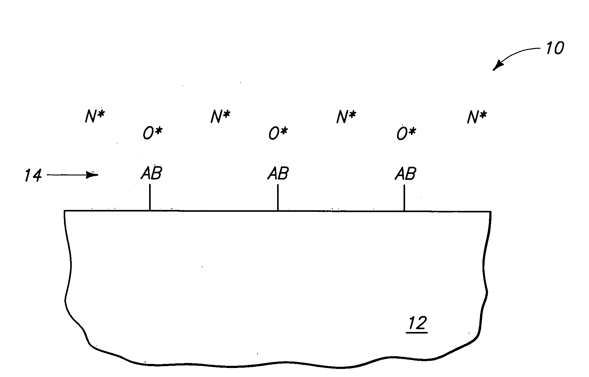
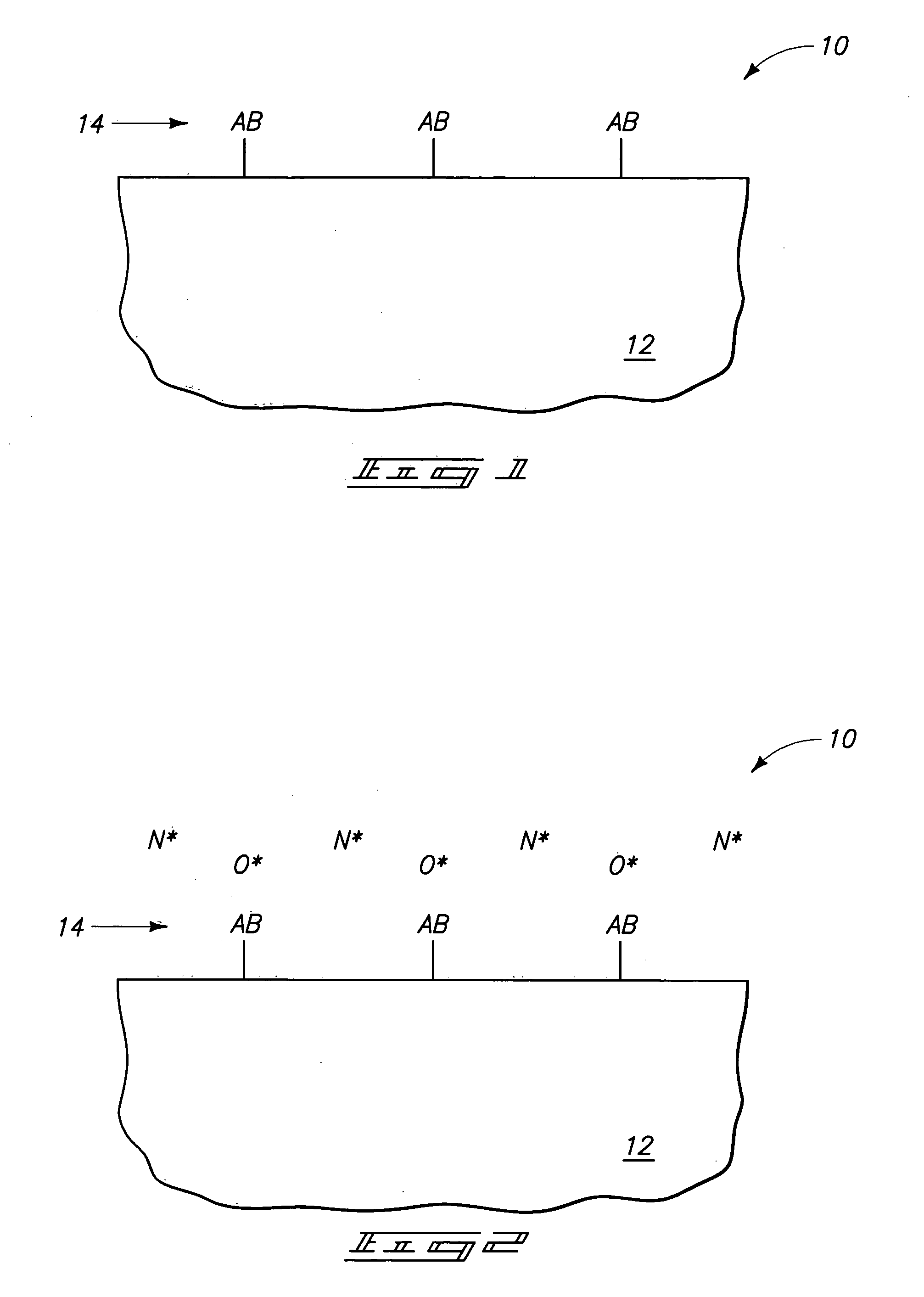
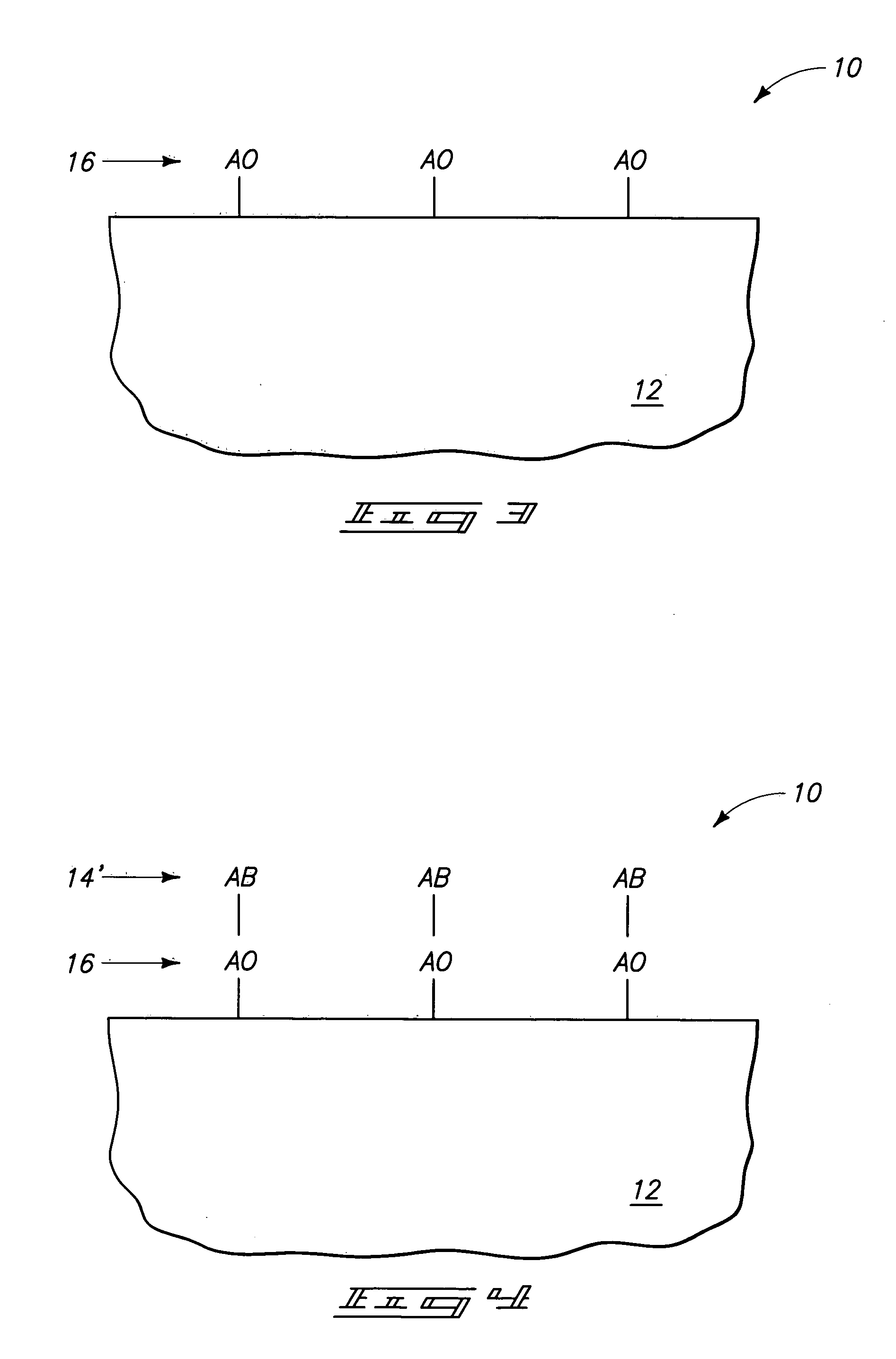
[0024] The invention comprises atomic layer deposition methods of depositing oxides on substrates. Atomic layer depositing (ALD) typically involves formation of successive atomic layers on a substrate. Described in summary, ALD includes exposing an initial substrate to a first chemical species to accomplish chemisorbtion of the species onto the substrate. Theoretically, the chemisorbtion forms a monolayer that is uniformly one atom or molecule thick on the entire exposed initial substrate. In other words, a saturated monolayer is preferably formed. Practically, chemisorbtion might not occur on all portions or completely over the desired substrate surfaces. Nevertheless, such an imperfect monolayer is still considered a monolayer in the context of this document. In many applications, mer...


PUM

PropertyMeasurementUnit
pressureaaaaaaaaaa
pressureaaaaaaaaaa
temperatureaaaaaaaaaa

Abstract

The invention includes atomic layer deposition methods of depositing an oxide on a substrate. In one implementation, a substrate is positioned within a deposition chamber. A first species is chemisorbed onto the substrate to form a first species monolayer within the deposition chamber from a gaseous precursor. The chemisorbed first species is contacted with remote plasma oxygen derived at least in part from at least one of O2 and O3 and with remote plasma nitrogen effective to react with the first species to form a monolayer comprising an oxide of a component of the first species monolayer. The chemisorbing and the contacting with remote plasma oxygen and with remote plasma nitrogen are successively repeated effective to form porous oxide on the substrate. Other aspects and implementations are contemplated.

Description

TECHNICAL FIELD [0001] This invention relates to atomic layer deposition methods of depositing an oxide on a substrate. BACKGROUND OF THE INVENTION [0002] Integrated circuits are typically formed on a semiconductor substrate such as a silicon wafer or other semiconductive material. In general, layers of various materials, which are one of semiconductive, conducting or insulating, are used to form the integrated circuits. By way of example, the various materials are doped, ion implanted, deposited, etched, grown, etc., using various processes. A continuing goal in semiconductor processing is to reduce the size of individual electronic components, thereby enabling smaller and denser integrated circuitry. [0003] As semiconductor devices continue to shrink geometrically, such has had a tendency to result in greater shrinkage in the horizontal dimension than in the vertical dimension. In some instances, the vertical dimension increases. Regardless, the result is increased aspect ratios (...

Claims


Application Information

Patent Timeline
Patent Type & Authority Applications(United States)
IPC IPC(8): C23C16/40C23C16/44C23C16/455
CPCC23C16/402C23C16/403C23C16/45542C23C16/45531C23C16/407
Inventor DERDERIAN, GARO J.MENG, SHUANGDYNKA, DANNY
Owner MICRON TECH INC
Why Eureka
Try Eureka