Substrate processing apparatus, control method for the apparatus, and program for implementing the method

Active Publication Date: 2005-06-09
TOKYO ELECTRON LTD
View PDF3 Cites 9 Cited by
  • Summary
  • Abstract
  • Description
  • Claims
  • Application Information

AI Technical Summary

Benefits of technology

[0016] It is an object of the present invention to provide a substrate processing apparatus, a control method for the apparatus, and a program for implementing the method

Problems solved by technology

Consequently, if the substrate processing apparatus continues to use the setup information for the dummy wafers in the FOUP 500 as it is, then confusion may arise.
However, the lifetime of a dummy wafer is approximately 1 to 2 weeks during mass production of semiconductor wafers, and in particular is only approximately 2 to 3 days in the case of inspection of processing in a corrosive system.
Under such a situation, there is a problem that if the setup information for the dummy wafers in the FOUP 500 is deleted from the HDDD or the like of the substrate processing apparatus, then the user must newly input/set setup information to the substrate processing apparatus every time dummy wafer replacement is carried out and hence there is a considerable burden on t

Method used


Image

  • Substrate processing apparatus, control method for the apparatus, and program for implementing the method
  • Substrate processing apparatus, control method for the apparatus, and program for implementing the method
  • Substrate processing apparatus, control method for the apparatus, and program for implementing the method

Examples


Embodiment Construction

[0040] The present invention will now be described in detail with reference to the drawings showing preferred embodiments thereof.

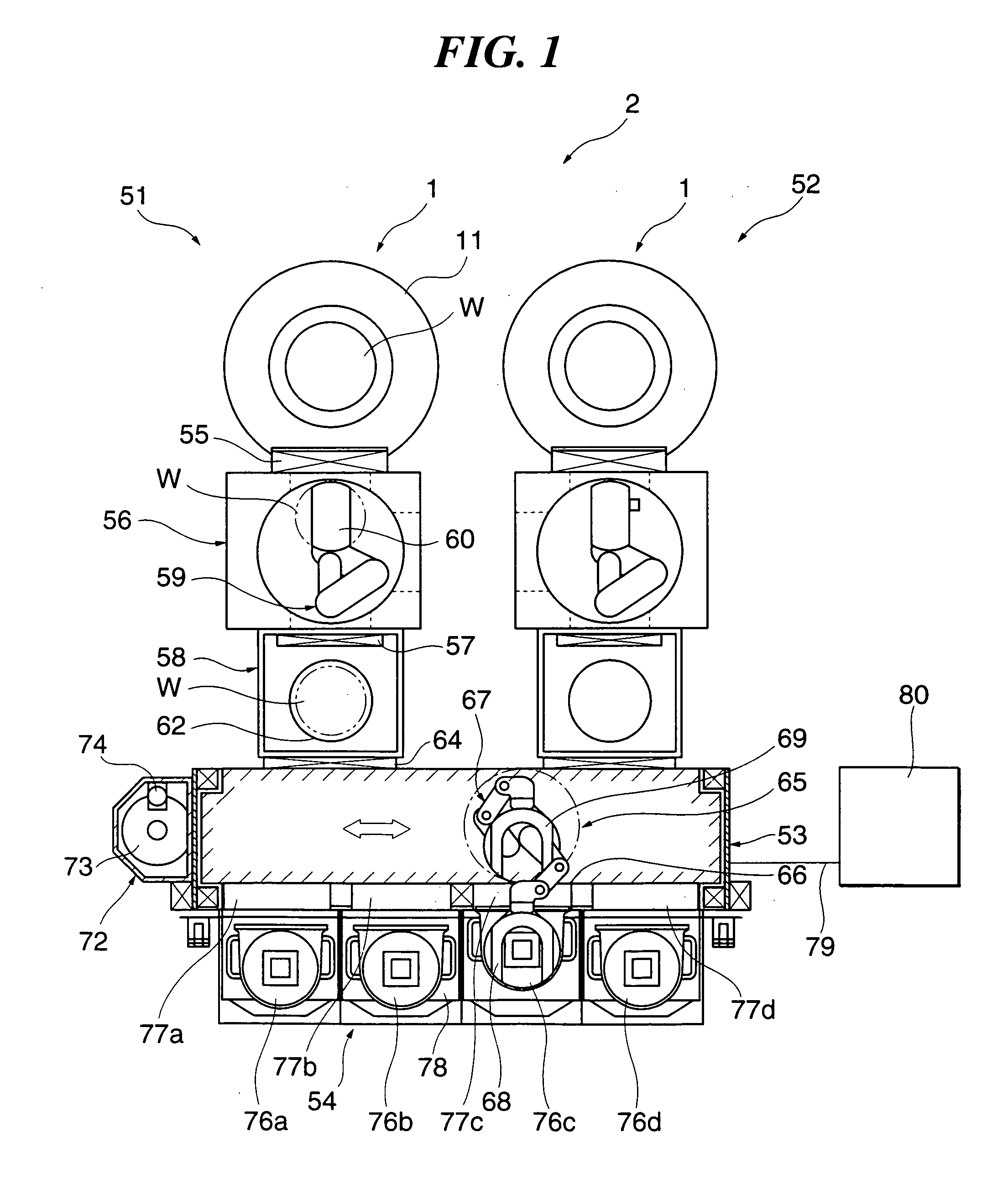
[0041]FIG. 1 is a plan view schematically showing the construction of a substrate processing apparatus according to an embodiment of the present invention.

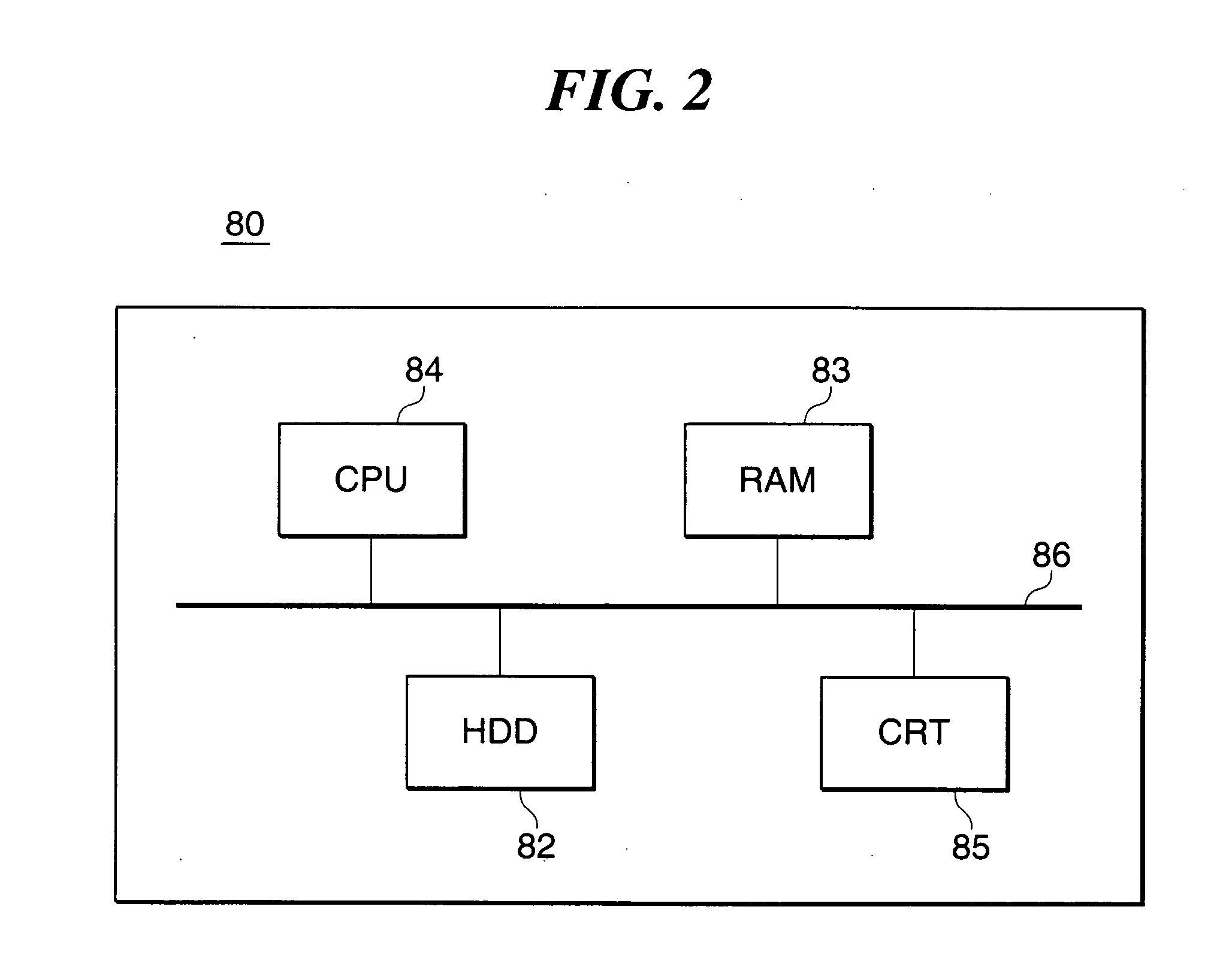
[0042] In FIG. 1, a plasma processing system 2, as the substrate processing apparatus according to the present embodiment, has a first processing unit 51 and a second processing unit 52 in which are carried out etching on semiconductor wafers W, a substrate transferring in / out stage 53, FOUP platforms 54 having FOUPs mounted thereon, and a control unit 80 that controls the operation of the plasma processing system 2.

[0043] The first processing unit 51 is comprised of a plasma processing apparatus 1 having a processing chamber 11 in which etching is carried out on the semiconductor wafers W, a transfer chamber 56 that is connected to the processing chamber 11 of the plasma processing apparatus 1 via a...


PUM

PropertyMeasurementUnit
Lifetime stabilityaaaaaaaaaa

Abstract

A substrate processing apparatus, according to which inspection of various devices in the substrate processing apparatus can be carried out with improved reliability, while reducing the burden on a user. A processing chamber processes semiconductor wafers therein. A transfer chamber transfers the semiconductor wafers. A FOUP (front opening unified pod) houses a plurality of dummy wafers for inspection of the processing chamber or the transfer chamber. A CPU causes an HDD (hard disk drive) to store a housing state relating to the arrangement of the dummy wafers in the FOUP before replacement of dummy wafers in the FOUP and that after the replacement as dummy wafer setup information.

Description

BACKGROUND OF THE INVENTION [0001] 1. Field of the Invention [0002] The present invention relates to a substrate processing apparatus that carries out processing on substrates as objects to be processed, a control method for the apparatus, and a program for implementing the method, and in particular relates to a substrate processing apparatus that carries out processing on dummy wafers, a control method for the apparatus, and a program for implementing the method. [0003] 2. Description of the Related Art [0004] Conventionally, in the manufacture of substrates (objects to be processed) for flat panel displays, semiconductor wafers and so on, substrate processing apparatuses comprised of at least one load lock chamber, at least one transfer chamber, and at least one processing chamber have been used to carry out various types of processing such as film formation, oxidation, diffusion, etching, and annealing. As such substrate processing apparatuses,.at least the two types described be...

Claims


Application Information

Patent Timeline
IPC IPC(8): H01L21/00H01L21/02
CPCH01L21/67294H01L21/67276Y10S414/135
Inventor SHIMIZU, NORIAKINUMAKURA, MASAHIRO
Owner TOKYO ELECTRON LTD
Why Eureka
Try Eureka