Dynamically reconfigurable logic circuit device, interrupt control method, and semi-conductor integrated circuit

Inactive Publication Date: 2005-06-09
PANASONIC CORP
View PDF6 Cites 13 Cited by
  • Summary
  • Abstract
  • Description
  • Claims
  • Application Information

AI Technical Summary

Benefits of technology

[0014] In view of the above, an object of the present invention is to provide a dynamically reconfigurable logic circu

Problems solved by technology

However, it takes some time to complete such a connection change.
In addition, it is difficult that the FPGA as well as the PLD changes the connections, in the course of treating another task, to provide different logic configurations.
However, the currently available dynamically reconfigurable logic circuit devices as represented by the disclosed dynamically reconfigurable logic circuit device require several clock periods to perform processing.
This requirement is incurred by the structural disadvantage of many arithmetic processing steps from input to output.
The structural disadvantage precludes high-speed processing to be carried out by the dynamically reconfigurable logic circuit devices, and each of the currently available dynamically reconfigurable logic circuit devices is slower in action than clock-synchronized, neighboring circuits.
General-purpose processors such as DSP and CPU are highly re-p

Method used


Image

  • Dynamically reconfigurable logic circuit device, interrupt control method, and semi-conductor integrated circuit
  • Dynamically reconfigurable logic circuit device, interrupt control method, and semi-conductor integrated circuit
  • Dynamically reconfigurable logic circuit device, interrupt control method, and semi-conductor integrated circuit

Examples


Example

First Embodiment

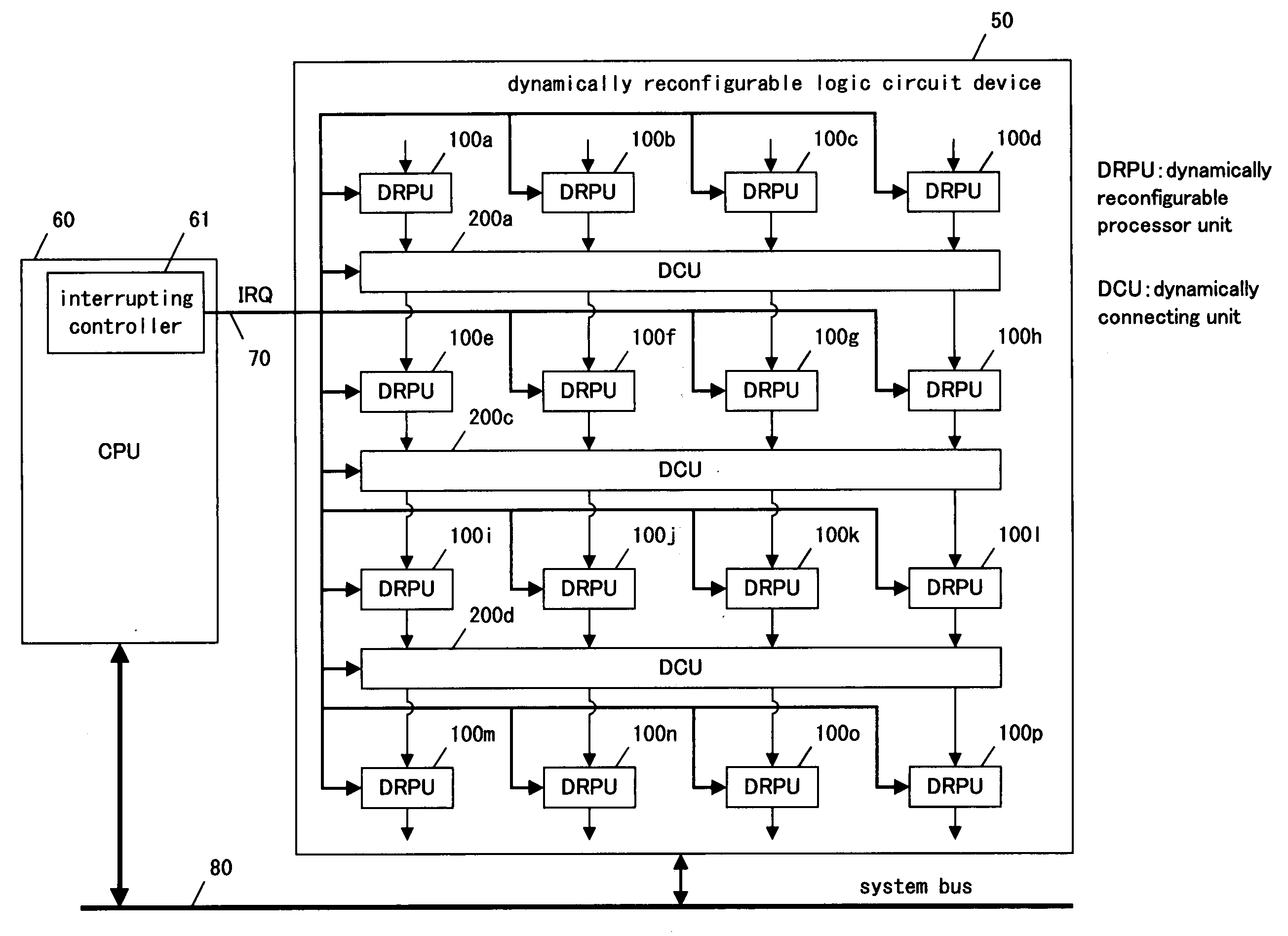
[0056]FIG. 1 shows a block diagram illustrating a dynamically reconfigurable logic circuit device according to a first embodiment and a related part of a semi-conductor integrated circuit incorporating the dynamically reconfigurable logic circuit device. The related part of a semi-conductor integrated circuit includes a CPU 60, the dynamically reconfigurable logic circuit device 50, and a system buss 80. The CPU 60 includes an interrupting controller 61. The interrupting controller 61 is operable to transmit an interrupting signal (IRQ) 70 to the dynamically reconfigurable logic circuit device 50. Data are transferred through the system buss 80 between the dynamically reconfigurable logic circuit device 50 and the CPU 60 and other units (not shown) of the semi-conductor integrated circuit.

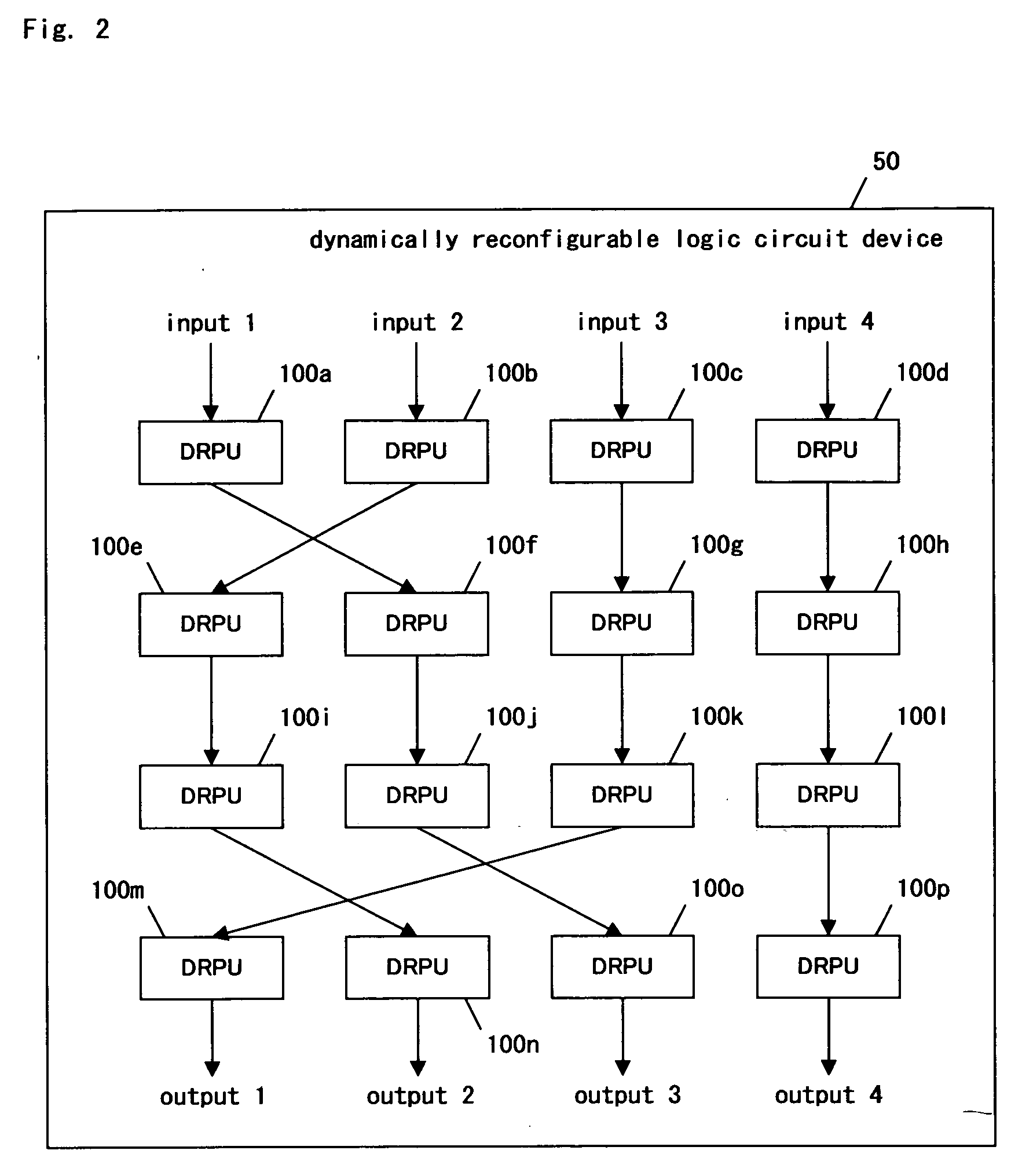
[0057] The dynamically reconfigurable logic circuit device 50 includes a plurality of dynamically reconfigurable processor units (DRPU) “100a” to “100p” arranged in array (hereina...

Example

Second Embodiment

[0067] Referring to FIG. 4, a dynamically reconfigurable processor unit 100 according to a second embodiment as illustrated in block diagram form is shown including a pair of setting registers “101a”, “101b”, a pair of flip-flops “102a”, “102b”, a pair of flip-flops “104a”, “104b”, computing devices 103, 105, and 106, a pair of flip-flops “107a”, “107b”, a pair of input data-switching units 108, 109, and an output data-switching unit 110. The computing devices 103, 105 are operable to perform either shift or mask operation. The computing device 106 is operable to perform addition and subtraction. The dynamically reconfigurable processor unit 100 according to the present embodiment further may include two different data inputs, i.e., a data input (DataIn0) 111 and a data input (dataIn1) 112, and a single data output (DataOut) 113.

[0068] The setting registers “101a”, “101b” serve as setting information storage units. The computing devices 103, 105, and 106 function ...

Example

Third Embodiment

[0088] Referring to FIG. 6, a dynamically connecting unit 200 according to a third embodiment as illustrated in block diagram form is of the two-input / four-output type, and is shown including a set of selectors 221, 222, 223, and 224, a pair of connection registers “230a”, “230b”, and a single selector 225. The selectors 221, 222, 223, and 224 are operable to select connections between inputs and outputs of the dynamically connecting unit 200, and consequently serve as connecting units. The connection registers “230a”, “230b” function as connection information storage units operable to store connection information. The selector 225 is operable to select between the connection registers “230a” and “230b”.

[0089] In usual processing, the selector 225 selects the connection register “230a”, and selects respective connections of the selectors 221, 222, 223, and 224 in accordance with the connection information in the connection register “230a”. For example, the selector...


PUM


Abstract

A dynamically reconfigurable logic circuit device includes a plurality of dynamically reconfigurable processor units (DRPU) arranged in array, and a plurality of dynamically connecting units (DCU). The dynamically connecting units interconnect inputs and outputs of the dynamically reconfigurable processor units. Each of the dynamically reconfigurable processor units includes a plurality of arithmetic processing configurations, a plurality of input data storage units, and a plurality of output data storage units. The arithmetic processing configurations, input data storage units, and output data storage units are both selected and set up in accordance with an interrupting signal from an interrupt controller. Similarly, the interconnection of the dynamically reconfigurable processor units through the dynamically connecting units is performed in accordance with the interrupting signal. The above structure is operable to change input data as well as the arithmetic processing configurations upon the issuance of a request for interrupt from a CPU, and to change the entire logic circuit configuration. As a result, time-division multiplexing is achievable.

Description

BACKGROUND OF THE INVENTION [0001] 1. Field of the Invention [0002] The present invention relates to a dynamically reconfigurable logic circuit device possessing a logic configuration dynamically changeable by programs, and an art related thereto, in particular, an art operable to change the logic configuration in response to an interrupting signal. [0003] 2. Description of the Related Art [0004] To successfully combine flexible software processing with high-speed hardware processing, a typical dynamically reconfigurable logic circuit device (in general called a dynamic reconfigurable logic or DRL) possessing a program-changeable logic configuration has recently been proposed. [0005] In the past, FPGA (a field programmable gate array) and PLD (a programmable logic device) are widely known as devices incorporating the program-changeable logic configurations. The FPGA and PLD are designed to dynamically change connections between transistors to a certain degree. However, it takes some...

Claims


Application Information

Patent Timeline
IPC IPC(8): G06F15/00G06F15/177G06F15/80H03K17/00H03K19/177
CPCG06F15/7867G06F15/177
Inventor KIMURA, TOMOO
Owner PANASONIC CORP
Why Eureka
Try Eureka