Transistor and semiconductor device

a technology of transistors and semiconductors, applied in the direction of transistors, semiconductor lasers, instruments, etc., can solve the problems of increasing the amount of energy consumption and the cost of backlight luminance, and achieve the effect of reducing the area of transistors, increasing the effective area of display portions, and high luminan

Inactive Publication Date: 2005-06-16
JAPAN SCI & TECH CORP
View PDF7 Cites 121 Cited by
  • Summary
  • Abstract
  • Description
  • Claims
  • Application Information

AI Technical Summary

Benefits of technology

[0003] Generally, the liquid crystal display device has been widely used for a notebook type personal computer or the like, and an energy-saving measure, a high luminance and a miniaturization have been requested of the liquid crystal display device. To reply to these requests, it is effective to increase a rate of an effective area of a display portion within a unit pixel. However, since a light shielding layer made of a metal thin film or the like in the transistor for driving the liquid crystal display device is formed as described above, a rate of an area of a light transmission portion to that of the light shielding layer (opening ratio) in the pixel reduces. Accordingly, a reduction of a transistor area by improving a performance of the transistor or an improvement of luminance of a backlight are necessary to develop a display device having high luminance. However, the measure to improve the characteristic of the transistor shows a limitation to a yield, leading to an increase in cost. Moreover, the measure to improve the luminance of the backlight increases an amount of energy consumption.
[0004] From the viewpoint of the above described points, the object of the present invention is to provide a transistor using a transparent channel layer made of zinc oxide or the like, which is transparent partially or entirely, because an orientation control of the zinc oxide and a valence electron control thereof that has been heretofore difficult is now possible. Specifically, the object of the present invention is to provide a transistor which uses a transparent material such as the zinc oxide or the like for a channel layer (conductive layer) so that the channel layer does not have a photosensitivity for the visible light region, and removes a necessity to form a light shielding layer, thus increasing an area rate of a display portion of a liquid crystal display device or the like.

Problems solved by technology

However, the measure to improve the characteristic of the transistor shows a limitation to a yield, leading to an increase in cost.
Moreover, the measure to improve the luminance of the backlight increases an amount of energy consumption.

Method used


Image

  • Transistor and semiconductor device
  • Transistor and semiconductor device
  • Transistor and semiconductor device

Examples


Embodiment Construction

(1) Field Effect Transistor (FET)

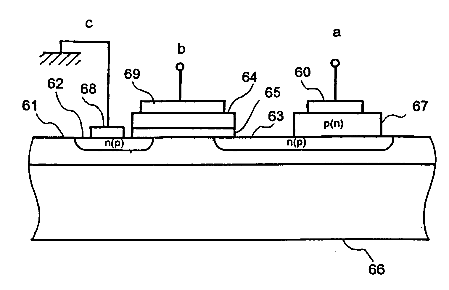
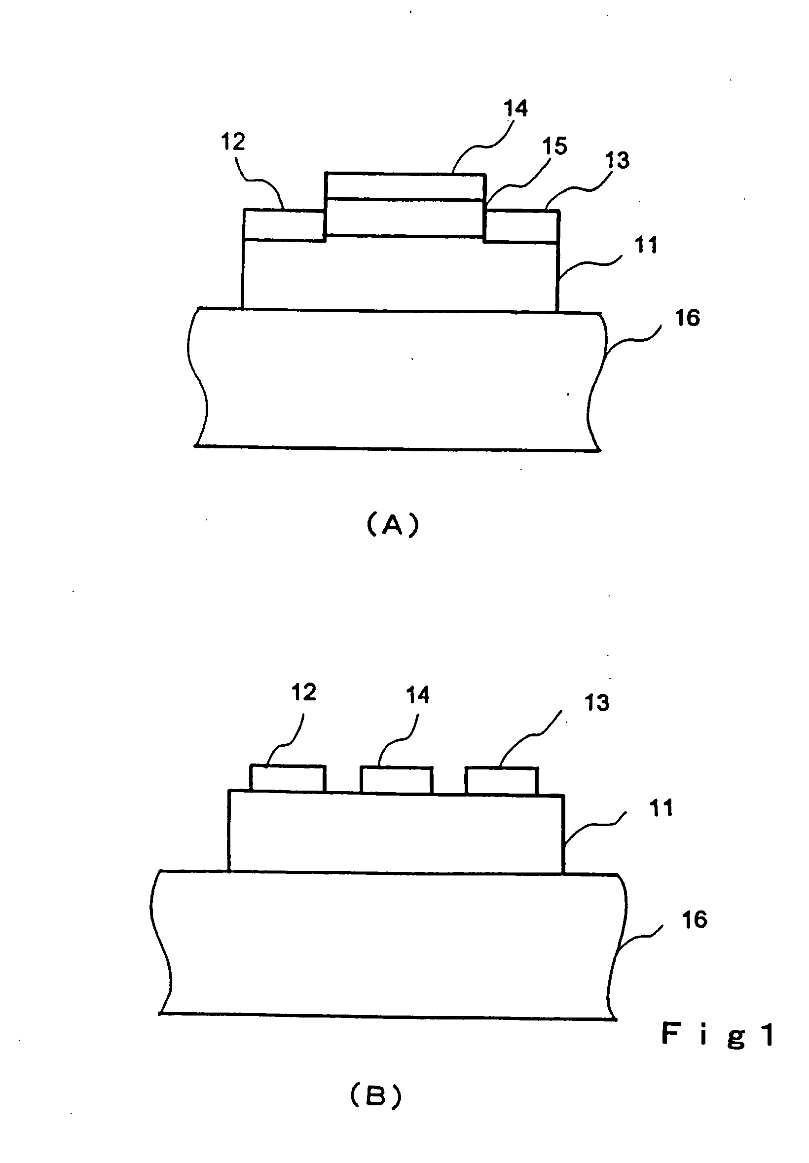
[0024] A section view of a first embodiment of a transistor according to the present invention is shown in FIGS. 1(A) and 1(B). As shown in FIG. 1(A), the transistor of the first embodiment relates to a FET, and comprises a channel layer 11, a source 12, a drain 13, a gate 14, a gate insulating layer 15 and a substrate 16. The channel layer 11 is formed on the substrate 16. On the channel layer 11, formed are the gate insulating layer 15, the source 12 and the drain 13. The gate 14 is formed on the gate insulating layer 15.

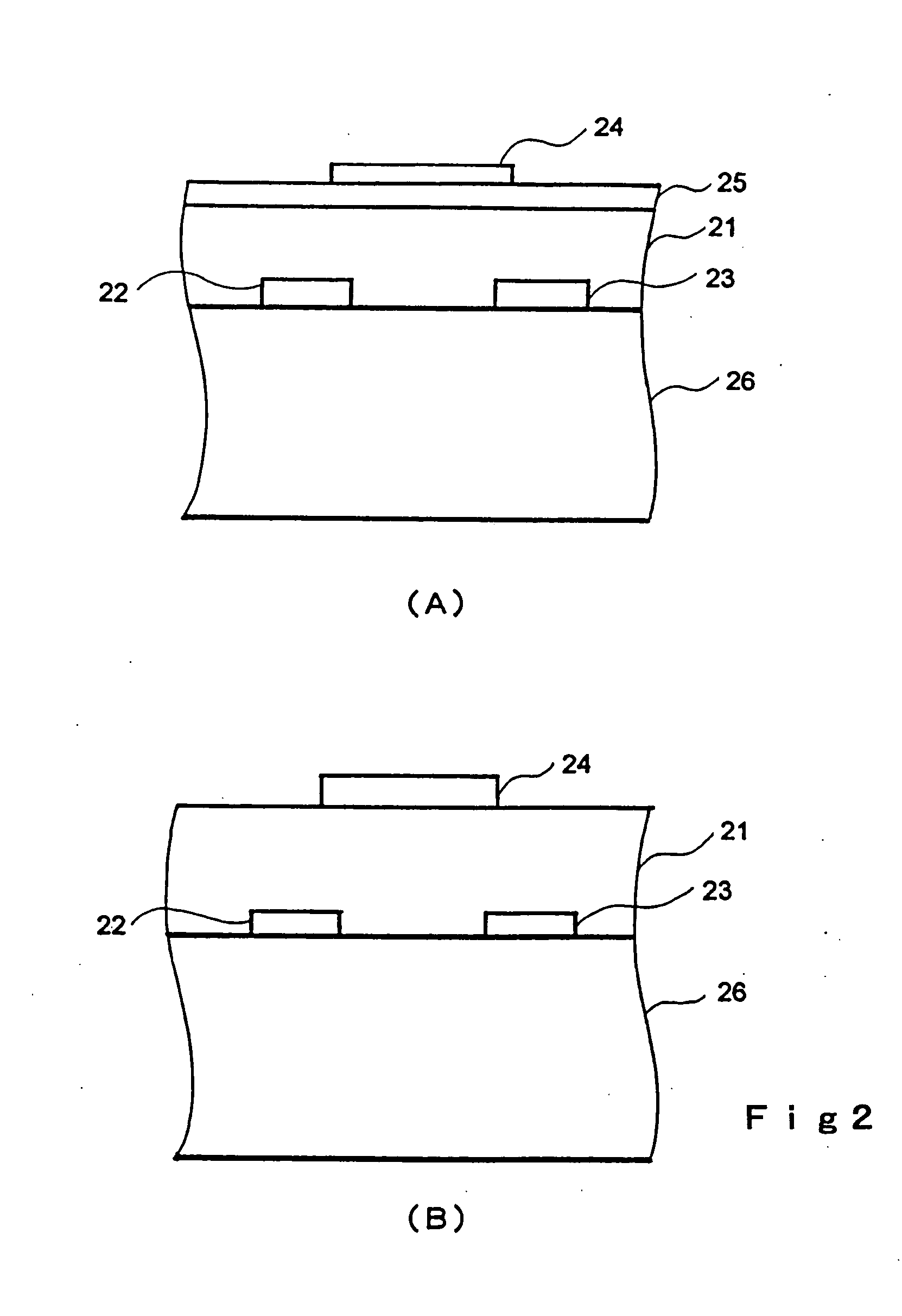
[0025] A modification of a first embodiment is shown in FIG. 1(B). In this transistor, the channel layer 11 is formed on the substrate 16. Furthermore, on the channel layer 11, the source 12 and the drain 13 are formed by an ohmic junction, and the gate 14 is formed thereon by a Shottky junction. In this embodiment, since the transistor lacks the gate insulating layer 15 unlike that of FIG. 1(A), a proper gap is provided between...


PUM


Abstract

A transistor is provided, which is entirely and partially transparent by the use of a transparent channel layer made of zinc oxide or the like. A channel layer 11 formed of a transparent semiconductor such as zinc oxide ZnO. A transparent electrode is used for all of a source 12, a drain 13 and a gate 14, or a part of them. As the transparent electrode, a transparent conductive material such as conductive ZnO doped with, for example, group III elements is used. As a gate insulating layer 15, a transparent insulative material such as insulative ZnO doped with elements capable of taking a valence of one as a valence number or group V elements is used. If a substrate 16 must be transparent, for example, glass, sapphire, plastic or the like can be used as a transparent material.

Description

FIELD OF THE INVENTION [0001] The present invention relates to a transistor and a semiconductor device, more particularly to a transparent transistor, a semiconductor device having the transparent transistor stacked thereon, and a semiconductor device to which the transparent transistor is applied for driving a light emission device, for reading / writing data from / to a memory, and for other purposes. It should be noted that in the present invention, a concept of “transparent” includes a concept of “being transparent or offering light transmission property” for the sake of simplifying descriptions. DESCRIPTIONS OF THE RELATED ARTS [0002] A thin film transistor using amorphous silicon, polycrystalline silicon or the like has been generally used as a transistor for use in driving liquid crystal display devices. Since these materials exhibit photosensitivity for the visible light region, carriers are generated by a beam of light, and resistivity of a thin film constituting the thin film ...

Claims


Application Information

Patent Timeline
Patent Type & Authority Applications(United States)
IPC IPC(8): G11C11/401H01L21/331H01L27/15H01L29/22H01L29/51H01L29/73H01L29/78H01L29/786H01L33/28H01S5/026
CPCH01L27/15H01L29/22H01L29/517H01L29/7317H01L29/78618H01L29/7869H01L33/28H01S5/0261H01L29/78H01L29/45H01L29/4908H01L29/80
Inventor KAWASAKI, MASASHIOHNO, HIDEO
Owner JAPAN SCI & TECH CORP
Why Eureka
Try Eureka