Basic cells configurable into different types of semiconductor integrated circuits

a technology of integrated circuits and basic cells, applied in logic circuits using elementary logic circuit components, logic circuits using specific components, pulse techniques, etc., can solve the problems of poor use efficiency of elements within basic cells, inability to finely adjust vth and tpd, and low frequency of use of nmos transistors. to achieve the effect of improving the efficiency of use of elements

Inactive Publication Date: 2005-06-16
LAPIS SEMICON CO LTD
View PDF8 Cites 26 Cited by
  • Summary
  • Abstract
  • Description
  • Claims
  • Application Information

AI Technical Summary

Benefits of technology

[0031] Hence one object of this invention is to improve the efficiency of use of elements in basic cells, and to enable fine adjustments to Vth and Tpd.

Problems solved by technology

Hence, as shown in FIG. 37 and FIG. 40, the frequency of use of the NMOS transistor is low compared with the PMOS transistors, and so usage efficiency of elements within the basic cell is poor.
Further, in a conventional basic cell the gate length and gate width are fixed, so that fine adjustments to Vth and Tpd cannot be made.
In particular, recently there have been increasingly frequent cases of special I / O cells developed using gate arrays; the inability to make fine adjustments to dimensions is a disadvantage.

Method used


Image

  • Basic cells configurable into different types of semiconductor integrated circuits
  • Basic cells configurable into different types of semiconductor integrated circuits
  • Basic cells configurable into different types of semiconductor integrated circuits

Examples


first embodiment

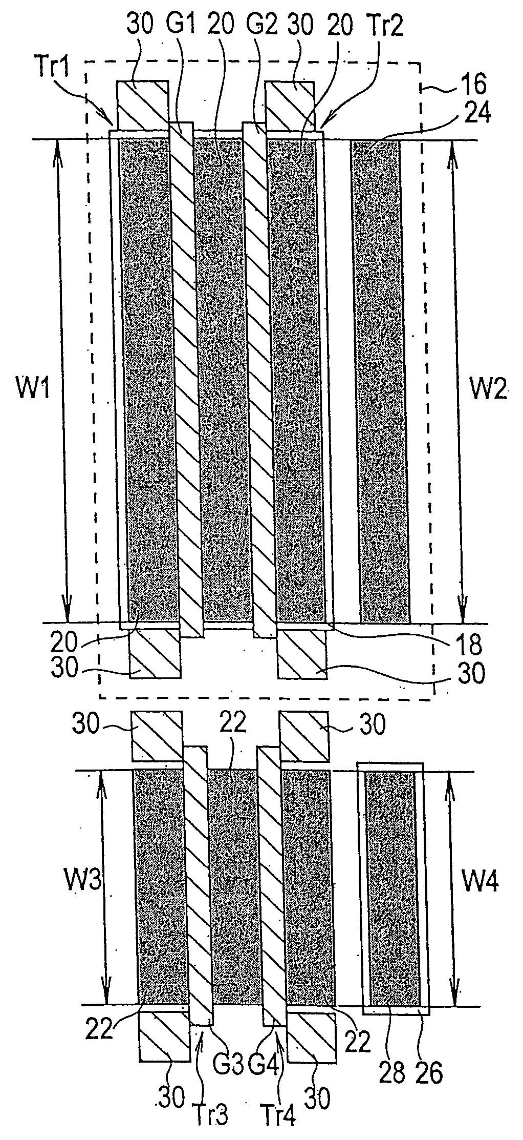
[0108]FIG. 1 is a mask pattern diagram of a basic cell comprised by a semiconductor integrated circuit of a first embodiment of this invention. The basic cell shown in FIG. 1 comprises a first P-channel MOS (hereafter “PMOS”) transistor Tr1, a second PMOS transistor Tr2, a first N-channel MOS (hereafter “NMOS”) transistor Tr3, and a second NMOS transistor Tr4.

[0109] Each of the transistors Tr1 through Tr4 is formed on P-type Si substrate, not shown. PMOS transistors Tr1 and Tr2 are formed within an N-well 16 formed in the substrate. Within this N-well 16, a P-type semiconductor region 18 is formed. Within this P-type semiconductor region 18, the active regions 20 of the PMOS transistors Tr1 and Tr2 are formed. Also, two parallel stripe-shape polysilicon films are formed on these active regions 20 as the gates G1 and G2 of the PMOS transistors Tr1 and Tr2.

[0110] Adjacent to the N-well 16, the active regions 22 of the NMOS transistors Tr3 and Tr4 are formed. On these active regions ...

second embodiment

[0139]FIG. 9 is a mask pattern diagram showing a basic cell comprised by the semiconductor integrated circuit of a second embodiment. The basic cell shown in FIG. 9 comprises a first PMOS transistor Tr1, a second PMOS transistor Tr2, a third PMOS transistor Tr3, a first NMOS transistor Tr4, and a second NMOS transistor Tr5.

[0140] Each of the transistors Tr1 through Tr5 is formed on P-type Si substrate, not shown. PMOS transistors Tr1, Tr2 and Tr3 are formed within an N-well 16 formed in the substrate. Within this N-well 16, a P-type semiconductor region 18 is formed. Within this P-type semiconductor region 18, the active regions 20 of the PMOS transistors Tr1, Tr2 and Tr3 are formed. Also, two parallel stripe-shape polysilicon films are formed on these active regions 20 as the gates G1, G2 and G3 of the PMOS transistors Tr1, Tr2 and Tr3. One of the polysilicon films is used as the gate G1 of PMOS transistor Tr1, and the other polysilicon film is used as the gates G2 and G3 of PMOS ...

third embodiment

[0162]FIG. 14 is a mask pattern diagram showing a basic cell comprised by the semiconductor integrated circuit of a third embodiment. The basic cell shown in FIG. 14 comprises a first PMOS transistor Tr1, a second PMOS transistor Tr2, a third PMOS transistor Tr3, a fourth PMOS transistor Tr4, a first NMOS transistor Tr5, and a second NMOS transistor Tr6.

[0163] Each of the transistors Tr1 through Tr6 is formed oh P-type Si substrate, not shown. PMOS transistors Tr1 through Tr4 are formed within an N-well 16 formed in the substrate. Within this N-well 16, a P-type semiconductor region 18 is formed. Within this P-type semiconductor region 18, the active regions 20 of the PMOS transistors Tr1 through Tr4 are formed. Also, two parallel stripe-shape polysilicon films are formed on these active regions 20 as the gates G1, G2, G3 and G4 of the PMOS transistors Tr1 through Tr4. One of the polysilicon films is used as the gates G1 and G3 of PMOS transistors Tr1 and Tr3, and the other polysil...


PUM


Abstract

The basic cell constituted by a semiconductor integrated circuit comprises two PMOS transistors and two NMOS transistors. By setting the gate widths of the gates of these transistors to prescribed lengths, the efficiency of use of elements within the basic cell is improved, and fine adjustment of the threshold voltage Vth and delay time Tpd becomes possible.

Description

BACKGROUND OF THE INVENTION [0001] 1. Field of the Invention [0002] This invention concerns a semiconductor integrated circuit comprised of macrocells prepared in advance, such as gate arrays. [0003] 2. Description of Related Art [0004] LSI manufacturing processes are divided into bulk processes, in which transistors, resistances and other elements are formed at prescribed positions on silicon substrate, and wiring processes, in which elements are connected by metal wiring to form circuit functions. In a gate array, the above-mentioned bulk processes are used to form in advance a bulk chip on which are regularly arranged basic cells (also called unit cells) in an array, so that, simply by changing the wiring processes, various logic circuits can be formed. [0005]FIG. 34 shows a bulk chip used to form the input / output circuit of a semiconductor integrated circuit. As shown in FIG. 34, in the case of an ordinary gate array, the input / output circuit (hereafter abbreviated to “I / O circu...

Claims


Application Information

Patent Timeline
Patent Type & Authority Applications(United States)
IPC IPC(8): H01L21/82H01L21/822H01L21/8234H01L21/8238H01L27/02H01L27/04H01L27/088H01L27/092H01L27/11H01L27/118H01L29/739H01L29/76H03K19/00H03K19/177
CPCH01L27/0207H01L27/092H01L27/11807Y10S257/903H03K19/0027H03K19/177H01L27/11898
Inventor SUSHIHARA, AKIHIRO
Owner LAPIS SEMICON CO LTD
Why Eureka
Try Eureka