Contactless mask programmable rom

a technology of programmable rom and contactless mask, which is applied in the direction of semiconductor devices, basic electric elements, electrical apparatus, etc., can solve the problem of complex fabrication process and achieve the effect of increasing device integration

Active Publication Date: 2005-06-16
SOLID STATE SYST
View PDF4 Cites 3 Cited by
  • Summary
  • Abstract
  • Description
  • Claims
  • Application Information

AI Technical Summary

Benefits of technology

[0015] Accordingly, this invention provides a contactless mask programmable read-only memory (Mask ROM) that contains no contact in the memory area and has a smaller memory array for increasing device integration.

Problems solved by technology

However, since an additional mask is needed for selectively implanting the channel regions of the memory cells 201, the fabricating process is more complex.

Method used


Image

  • Contactless mask programmable rom
  • Contactless mask programmable rom
  • Contactless mask programmable rom

Examples


Embodiment Construction

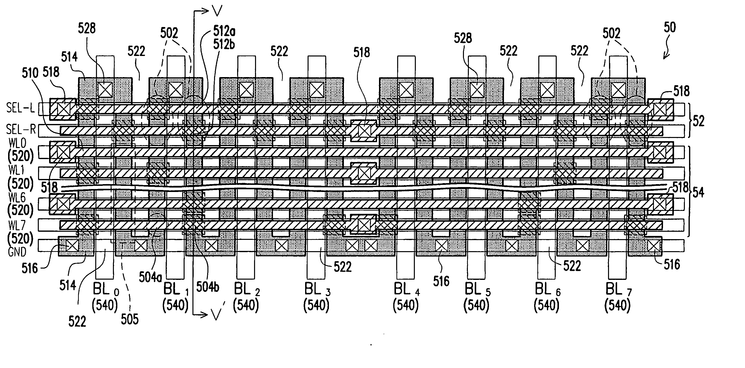
[0028]FIG. 4A illustrates a top view of a contactless Mask ROM according to an embodiment of this invention, and FIG. 4B illustrates a cross-sectional view of the same along line IV-IV′.

[0029] Referring to FIGS. 4A-4B, the contactless Mask ROM 400 comprises a plurality of word lines 420 extending in row direction, and rows and columns of N-type diffusions 440 located in a P-type substrate 402 (FIG. 4B). As shown in FIG. 4B, each word line 420 is isolated from the substrate 402 by gate dielectrics 404. The word lines 420 comprise a material such as doped polysilicon, and the N-type diffusions 440 are doped with phosphorous (P) or arsenic (As), for example. In the contactless Mask ROM 400, two columns of N-type diffusions 440 are separated by an isolation layer 410. Two rows of diffusions 440 are separated by a word line 420, and the two terminal diffusions 440 in each column of diffusions 440 are coupled to a bit line BLn) and ground, respectively. In addition, two adjacent diffusio...


PUM


Abstract

A contactless Mask ROM is described, comprising a plurality of MOS-type memory cells. The memory cells include a plurality of first memory cells and a plurality of second memory cells. The first memory cells have a first channel conductivity so that they are depletion-mode MOS transistors, and the second memory cells have a second channel conductivity so that they are enhanced-mode MOS transistors. In the contactless Mask ROM, a memory cell shares two diffusions with two adjacent memory cells that are aligned with the memory cell along a first direction.

Description

BACKGROUND OF THE INVENTION [0001] 1. Field of Invention [0002] The present invention relates to a semiconductor device. More particularly, the present invention relates to a contactless mask programmable read-only memory (Mask ROM). [0003] 2. Description of Related Art [0004] Read-only memory (ROM) is a type of non-volatile memory, which can retain data as disconnected from power supply, and therefore is used to store permanent data like booting data of computer systems. [0005] In order to simplify the fabricating processes and to increase the integration of ROM devices, various ROM structures are proposed based on shared diffusion and integration of the coding process and the contact process. Some conventional ROM devices are described below. [0006]FIG. 1 illustrates a top view of a contact ROM in the prior art. [0007] Referring to FIG. 1, the contact ROM 100 comprises rows and columns of MOS-type memory cells, wherein two adjacent memory cells in the same column constitute a cell...

Claims


Application Information

Patent Timeline
Patent Type & Authority Applications(United States)
IPC IPC(8): H01LH01L21/8238H01L21/8246H01L21/8247H01L27/112H01L27/115H01L29/76
CPCH01L27/112H01L27/1126H01L27/11233H01L27/11226H10B20/34H10B20/36H10B20/383H10B20/00
Inventor LIOU, JHYY-CHENGLIN, CHIN-HSI
Owner SOLID STATE SYST
Why Eureka
Try Eureka