P-channel NAND flash memory and operating method thereof

a technology of which is applied in the field of p-channel nand flash memory and operating method thereof, can solve the problems of low efficiency of electron injection, low efficiency of device miniaturization, and relatively high operating voltage, so as to improve the efficiency of memory cells, speed up the programming operation, and reduce the operating voltage

Active Publication Date: 2006-06-13
POWERCHIP SEMICON MFG CORP
View PDF2 Cites 5 Cited by
  • Summary
  • Abstract
  • Description
  • Claims
  • Application Information

AI Technical Summary

Benefits of technology

[0010]In view of the above, the present invention is directed to provide a p-channel NAND (Not-AND) flash memory and operating method thereof, so as to speed up the programming operation, lower the operating voltage, and increase the efficiency of the memory cells.
[0011]The present invention is further directed to provide a p-channel NAND flash memory and operating method thereof, so as to enhance the integration and reliability of the memory cells.
[0015]In the aforementioned p-channel NAND flash memory array, the erase gate is formed on the doped region (source / drain). Thus, the memory cells can draw electrons, via F-N tunneling during an erasing operation, from the floating gate into the erase gate for removal. In this manner of the erasing operation, the frequency for electrons passing through the tunneling dielectric layer can be lowered, and consequently lifetime of the tunneling dielectric layer can be extended, and reliability of the device can be enhanced.
[0016]In addition, in this invention every two adjacent stacked gate structures share one erase gate. Thus, increase in the size of the flash memory cells is not required, and accordingly, the integration of the device can be enhanced.
[0021]During the operations of NAND flash memory arrays according to this invention, band-to-band tunneling induced hot electron injection is utilized to cause electrons to pass through tunneling dielectric layer and enter into the floating gates, for programming operation of the memory cells; and F-N tunneling effect is utilized to cause electrons from the floating gates to pass through the inter-gate dielectric layer and enter into the erase gate, for erasing operation of the memory cells. Through the operations of this invention, since the frequency for electrons passing through the tunneling dielectric layer is lowered, the lifetime of the tunneling dielectric layer can be extended, and the reliability of the devices can be enhanced. In addition, since band-to-band tunneling induced hot electron injection, which has a high electron injecting efficiency, is utilized during the programming operation, amount of current in memory cells can be reduced, and thus the operating rate can be increased accordingly. Furthermore, since band-to-band tunneling induced hot electron injection and F-N tunneling effects are utilized during the programming and erasing operations, electricity usage is low, and thus power consumption of the entire memory device can be effectively reduced.

Problems solved by technology

For the CHEI, however, electron injection efficiency is low, and a relatively high operating voltage is required.
For the SSI, on the other hand, the size of the devices will be continuingly miniaturized and the coupling capacity between gates of the devices will be reduced with enhancement of the integration of the devices; thus, during a programming operation, the vertical electric field between the control gate and the substrate will be insufficient and thus to slow down the progress of the programming operation.
For an NAND array, however, the procedures of memory cells programming and data writing / erasing are more complicated.
Moreover, since many memory cells are in series connection in the array, electric current of reading operation for memory cells becomes weaker, which will slow down the operation of the memory cells, and adversely affect the efficiency of the entire device.

Method used


Image

  • P-channel NAND flash memory and operating method thereof
  • P-channel NAND flash memory and operating method thereof
  • P-channel NAND flash memory and operating method thereof

Examples


Embodiment Construction

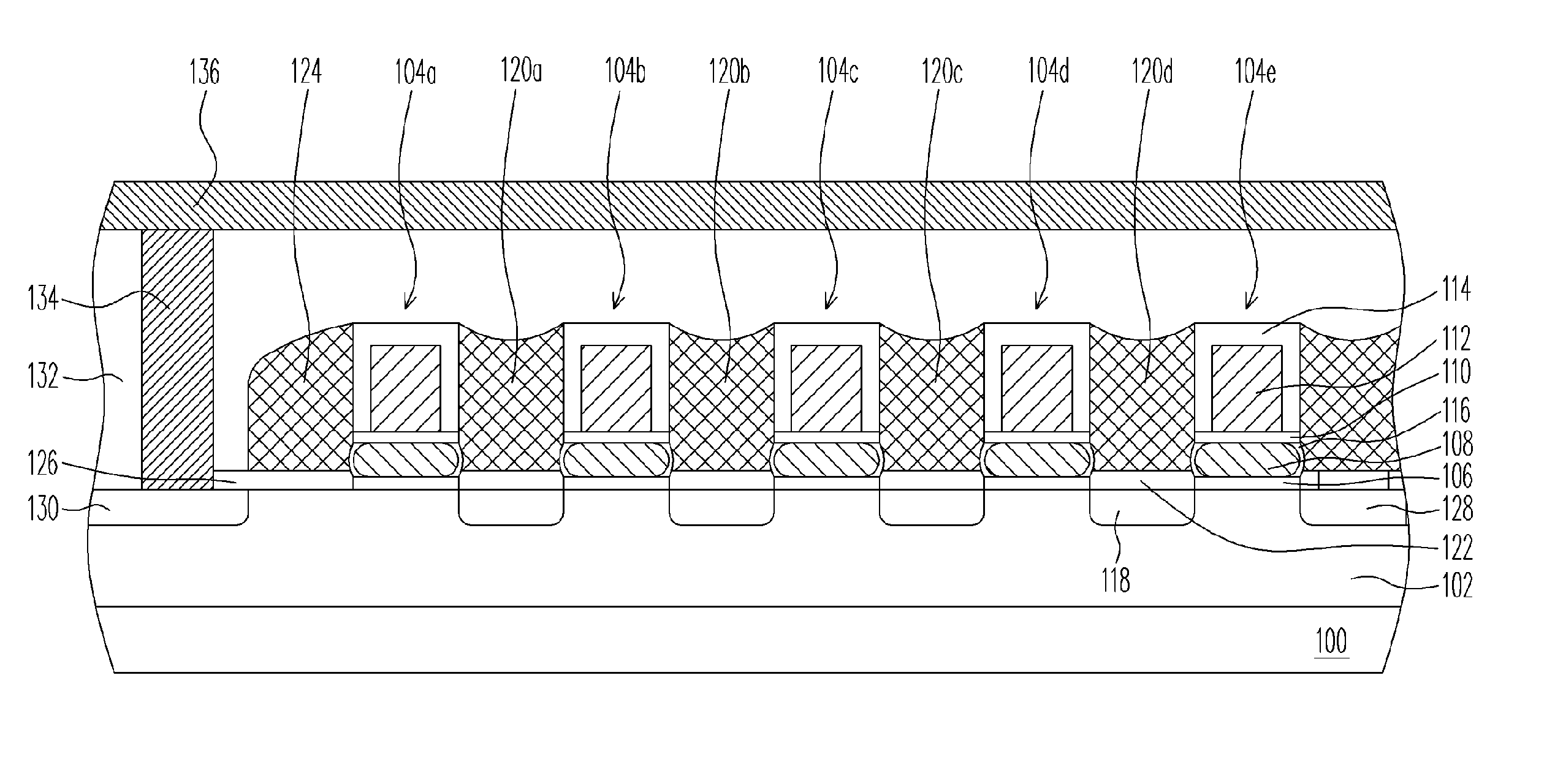
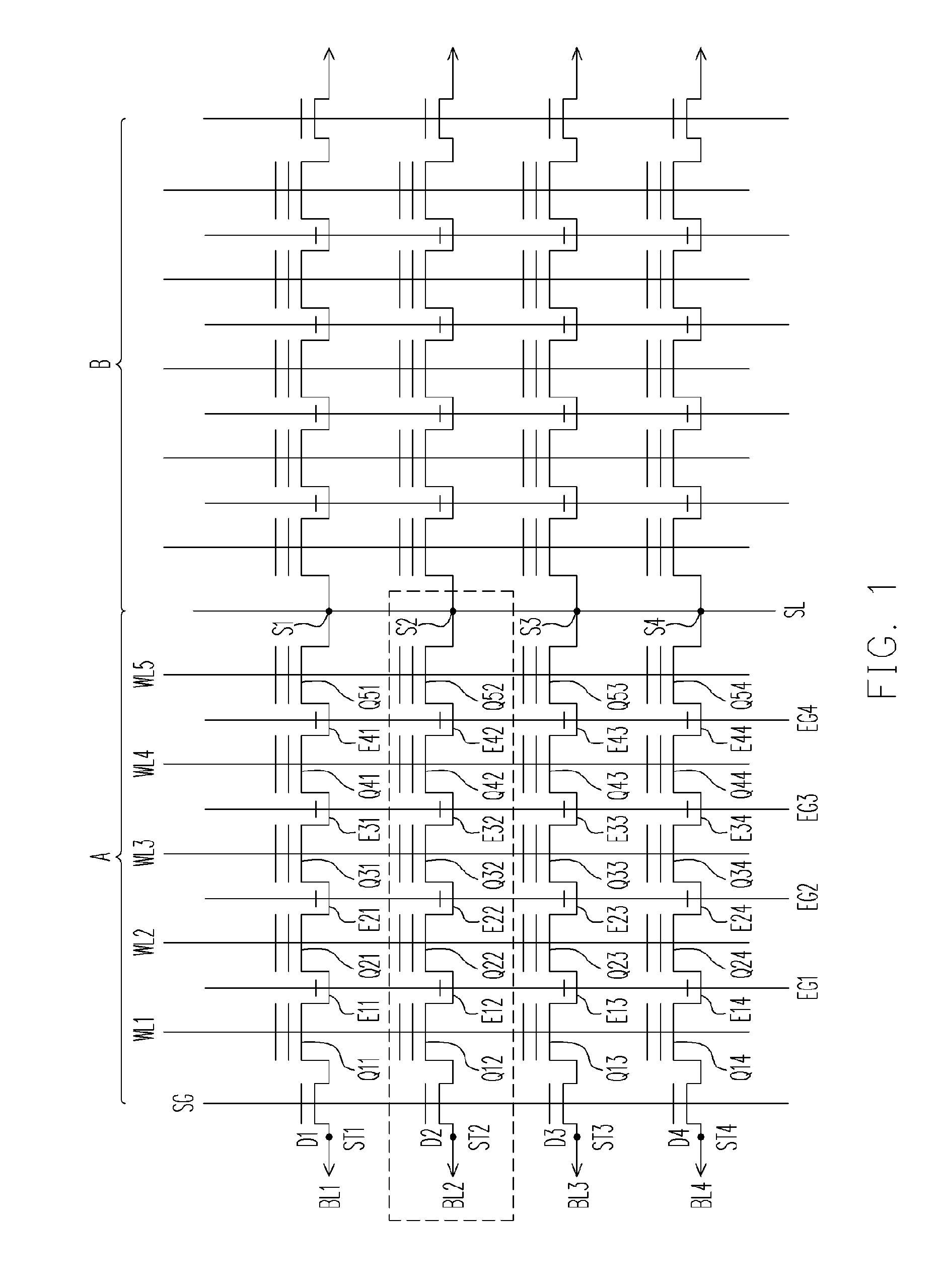
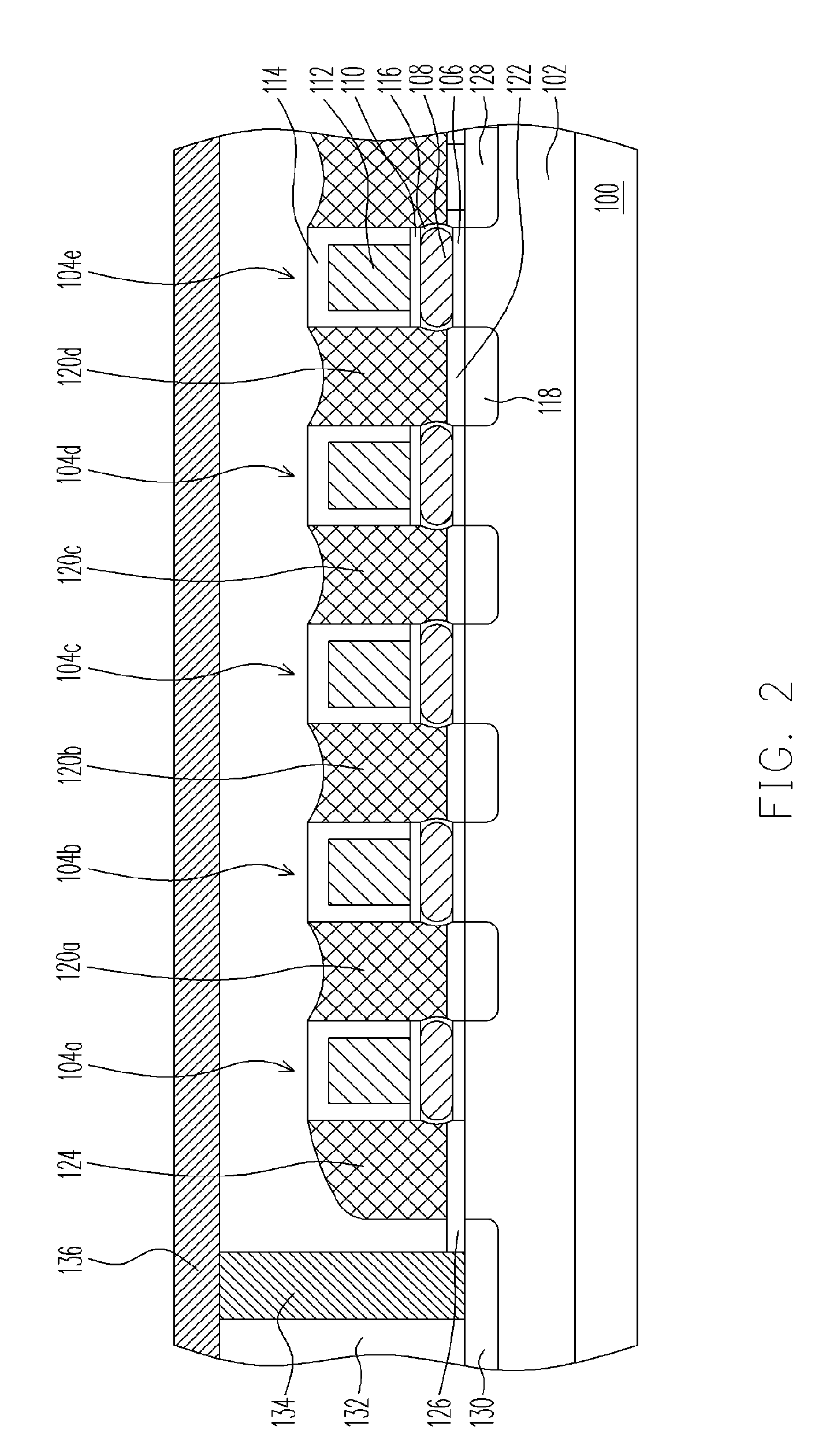
[0025]Reference will now be made in detail to the preferred embodiments of the invention. FIG. 1 is circuit diagram showing a p-channel NAND (Nor-AND gate) flash memory cell array. In this embodiment, a p-channel NAND memory cell array with four rows is illustrated as an example. In this invention, a one time programmable ROM contains memory array A and memory array B, wherein the memory arrays A and B share a source region (source line SL). Only memory array A is further described below since memory array B is structurally the same as memory array A.

[0026]Referring to FIG. 1, the p-channel NAND flash memory cell array contains a plurality of select transistors ST1˜ST4, a plurality of memory cells Q1˜D54, a plurality of word lines WL1˜WL5, a select gate line SG, a plurality of bit lines BL1˜BL4, and a plurality of erase gate lines EG1˜EG4.

[0027]The select transistor ST1 and memory cells Q11˜Q51 form a memory cell row in series connection between a drain region D1 and a source region...


PUM


Abstract

A p-channel NAND flash memory includes a plurality of memory cells in series connection between a p-type source region and a p-type drain region. Each memory cell includes a tunneling dielectric layer, a floating gate, and a control gate. An erase gate is formed between two adjacent memory cells, and a p-type doped region is formed in the substrate between two adjacent memory cells. A select transistor is formed between the p-type drain and the cell nearest to the p-type drain. The cells in the p-channel NAND flash memory is programmed by band-to-band tunneling induced hot carrier injection, and erased via F-N tunneling.

Description

CROSS-REFERENCE TO RELATED APPLICATION[0001]This application claims the priority benefit of Taiwan application serial no. 93134067, filed on Nov. 9, 2004. All disclosure of the Taiwan application is incorporated herein by reference.BACKGROUND OF THE INVENTION[0002]1. Field of the Invention[0003]The present invention relates to a semiconductor memory device, and more particularly to a p-channel NAND flash memory and operating method thereof.[0004]2. Description of the Related Art[0005]Flash memory devices are applicable for multiple operations of data writing, reading and erasing, and have the advantage that stored data will not been vanished even after power supply is cut off. Thus, flash memory devices are widely used as non-volatile memory devices for personal computers and other electronic facilities.[0006]In a conventional flash memory device, doped poly-silicon is used for fabricating floating gate and control gate. The control gate is formed directly on the floating gate, a di...

Claims


Application Information

Patent Timeline
Patent Type & Authority Patents(United States)
IPC IPC(8): G11C16/04G11C16/02G11C16/12H01L27/115
CPCG11C16/12G11C16/0483
Inventor HUNG, CHIH-WEIHSU, CHENG-YUAN
Owner POWERCHIP SEMICON MFG CORP
Why Eureka
Try Eureka