Method of improving device resistance

a technology of memory devices and resistance, applied in the direction of semiconductor devices, basic electric elements, electrical appliances, etc., can solve the problems of increasing the resistance reducing the current flow affecting the performance of the memory device, so as to achieve the effect of reducing the resistance of the bit lin

Inactive Publication Date: 2005-02-01
MACRONIX INT CO LTD
View PDF9 Cites 5 Cited by
  • Summary
  • Abstract
  • Description
  • Claims
  • Application Information

AI Technical Summary

Benefits of technology

Accordingly, the present invention provides a structure of a buried bit line of a memory device and a fabrication method thereof, wherein the bit line resistance is reduced.

Problems solved by technology

A narrower linewidth, however, would lead to its resistance to increase.
Consequently, the current flow of the memory device is reduced and bit line loading would become too high.
If the junction depth of the buried drain region is increased to resolve the problem of raised resistance at the linewidth, not only is the short channel effect generated, the problem of junction leakage also occurs.
If a high concentration of dopants is used to form a shallow junction of the bit line to obviate the short channel effect and the junction leakage problem due to a deep junction, the overloading problem of the bit line remains unresolved because of the limitation of the solid-phase solubility.
The formation of a bit line contact, however, is limited by the integration of the device.

Method used


Image

  • Method of improving device resistance
  • Method of improving device resistance
  • Method of improving device resistance

Examples


Embodiment Construction

In this aspect of the invention, the fabrication methods and the structures of a mask ROM device and a silicon nitride memory device are used illustrate the features of the invention. However, it should be appreciated that the teaching of the present invention is not limited to a mask ROM device or a silicon nitride memory device.

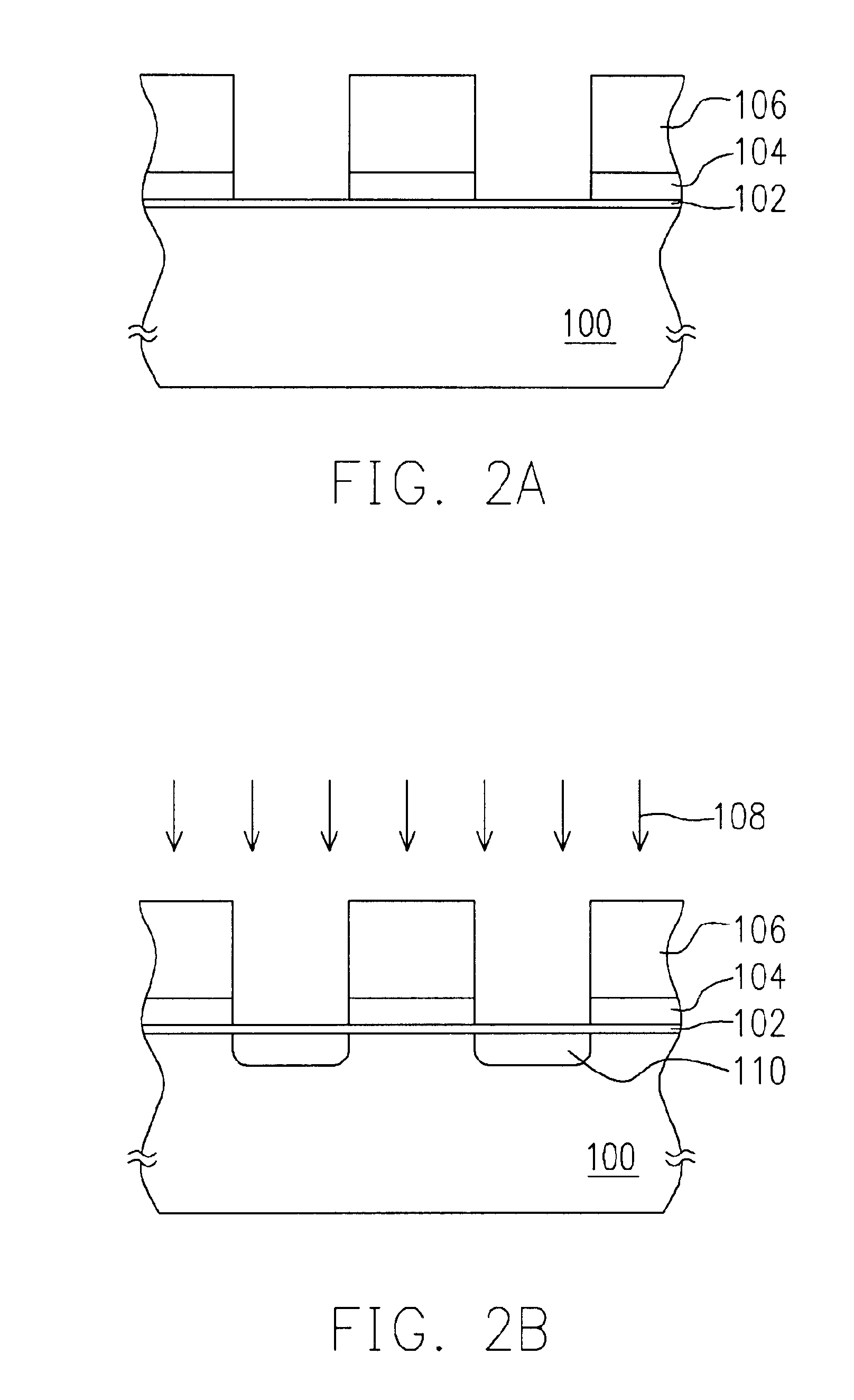
FIGS. 2A to 2F are schematic cross-sectional views illustrating the process flow for manufacturing of a memory device according to one aspect of the present invention.

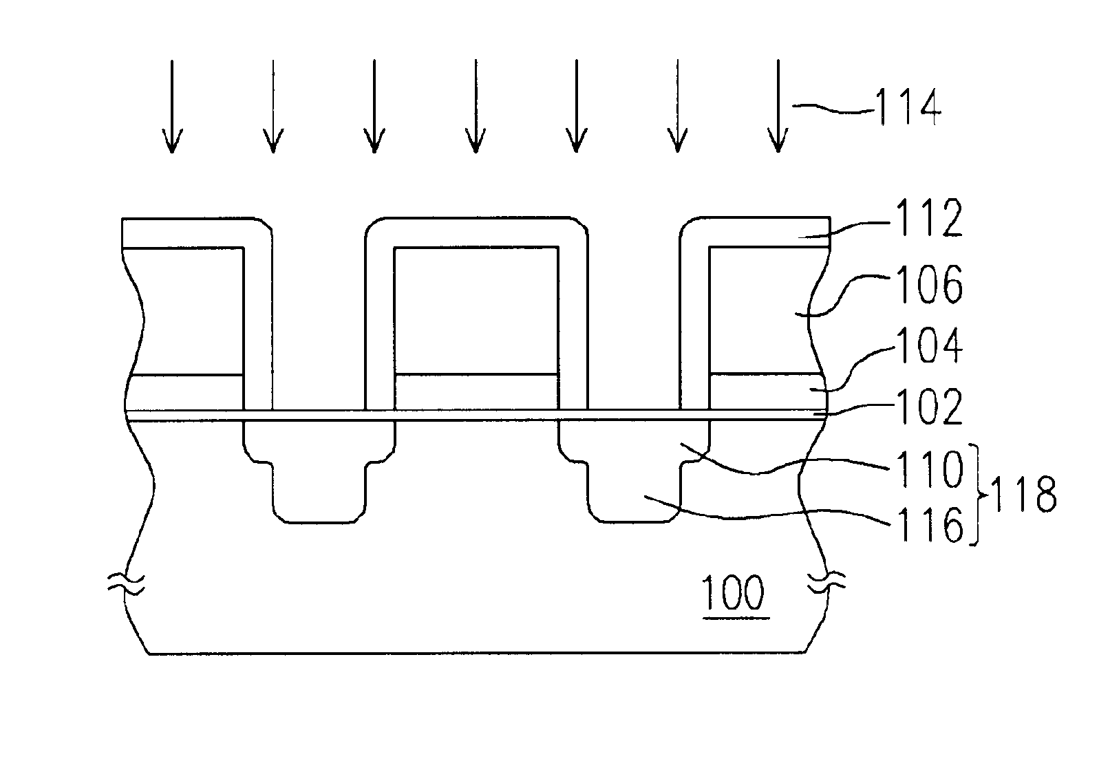
Referring to FIG. 2A, a pad oxide layer 102 is formed on a substrate 100 to protect the surface of the substrate 100. A patterned mask layer 106 is further formed on the pad oxide layer 102, wherein the mask layer 106 can be a photoresist layer, a polysilicon layer, or a dielectric material layer (for example, silicon nitride or silicon oxide type of dielectric material). In this aspect of the present invention, if the mask layer 106 is a photoresist material, an anti-reflection layer 104 is f...


PUM


Abstract

A buried bit line and a fabrication method thereof, wherein the device includes a substrate, a shallow doped region disposed in the substrate, a deep doped region disposed in the substrate below a part of the shallow doped region, wherein the shallow doped region and the deep dope region together form a bit line of the memory device.

Description

BACKGROUND OF INVENTION1. Field of the InventionThe present invention relates to a structure of a memory device and a fabrication method thereof. More particularly, the present invention relates to a structure of buried bit line of a memory device and a fabrication method thereof.2. Description of Related ArtMemory device, by nature, is a semiconductor device used to store information and data. The storage of digital information is in unit of bit. Information is stored in a cell in the memory device. The specific location of each memory cell is known as an address. In other words, the memory cells in a memory device are arranged in an array, wherein a specific row and column constitutes a specified memory cell address. The memory cells on each row or each column are connected with a common conductive line.Referring to FIG. 1, FIG. 1 is a schematic, cross-sectional view of a structure of a memory cell device according to the prior art.Referring to FIG. 1, a conventional memory device...

Claims


Application Information

Patent Timeline
Patent Type & Authority Patents(United States)
IPC IPC(8): H01L27/115H01L21/70H01L21/8246H01L21/768H01L27/10H01L27/112
CPCH01L27/11568H01L27/115H10B69/00H10B43/30
Inventor LAI, JIUN-RENYANG, CHUN-YICHEN, SHI-XIANCHANG, GWEN
Owner MACRONIX INT CO LTD
Why Eureka
Try Eureka