Method of fabricating T-shaped polysilicon gate by using dual damascene process

Inactive Publication Date: 2005-11-24
GRACE SEMICON MFG CORP
View PDF4 Cites 5 Cited by
  • Summary
  • Abstract
  • Description
  • Claims
  • Application Information

AI Technical Summary

Benefits of technology

[0007] The present invention provides a method of fabricating a T-shaped polysilicon gate by using dual damascene process, which effectively prevents low po

Problems solved by technology

However, in order to further shrink device dimensions, while performing the source/drain extension dopant process, t

Method used


Image

  • Method of fabricating T-shaped polysilicon gate by using dual damascene process
  • Method of fabricating T-shaped polysilicon gate by using dual damascene process
  • Method of fabricating T-shaped polysilicon gate by using dual damascene process

Examples


Embodiment Construction

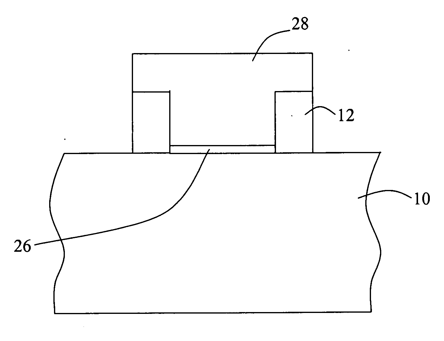
[0014] The present invention provides a method of fabricating a T-shaped polysilicon gate by using dual damascene process, as shown in FIGS. 1 through 7, which illustrate a T-shaped polysilicon gate according to a preferred embodiment of the present invention.

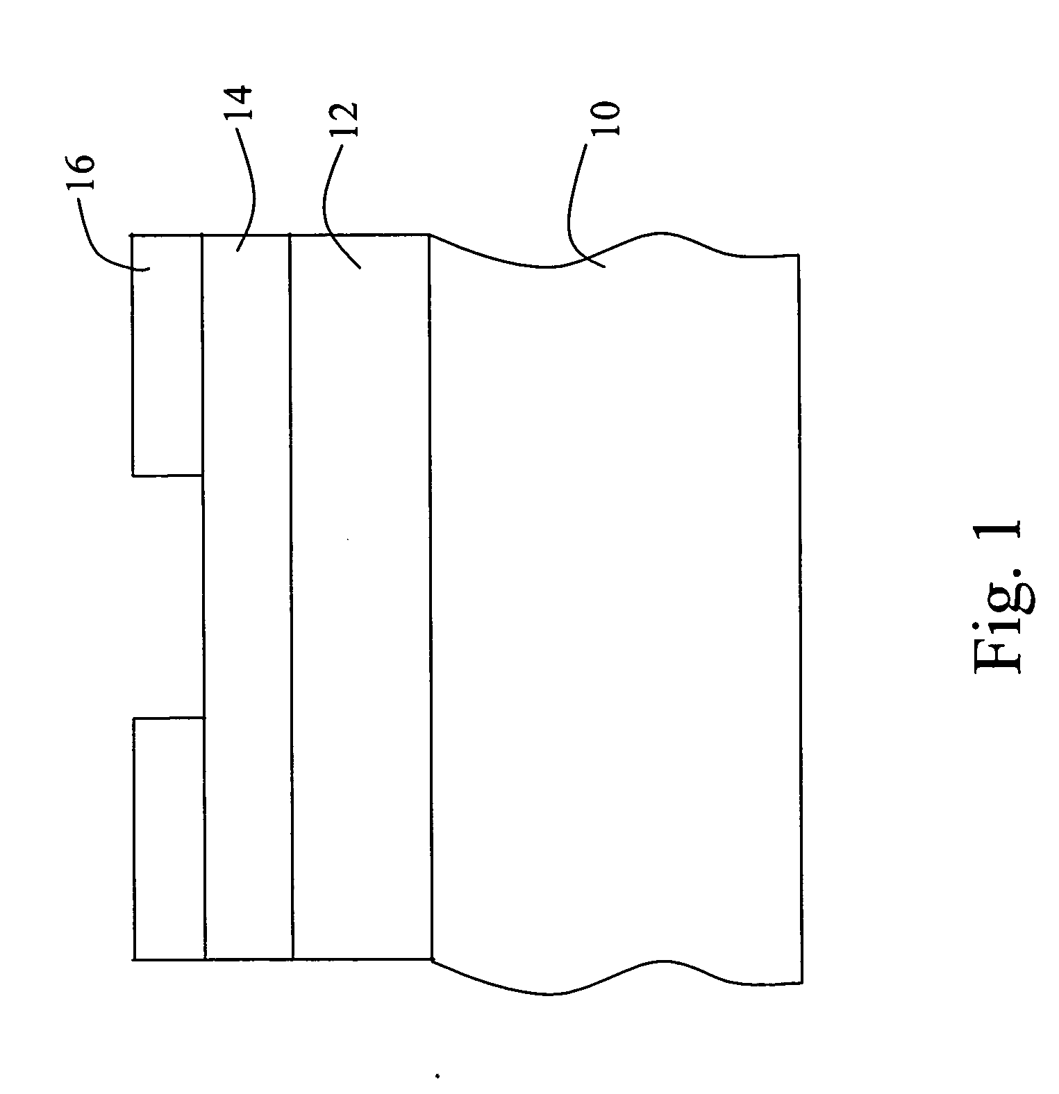
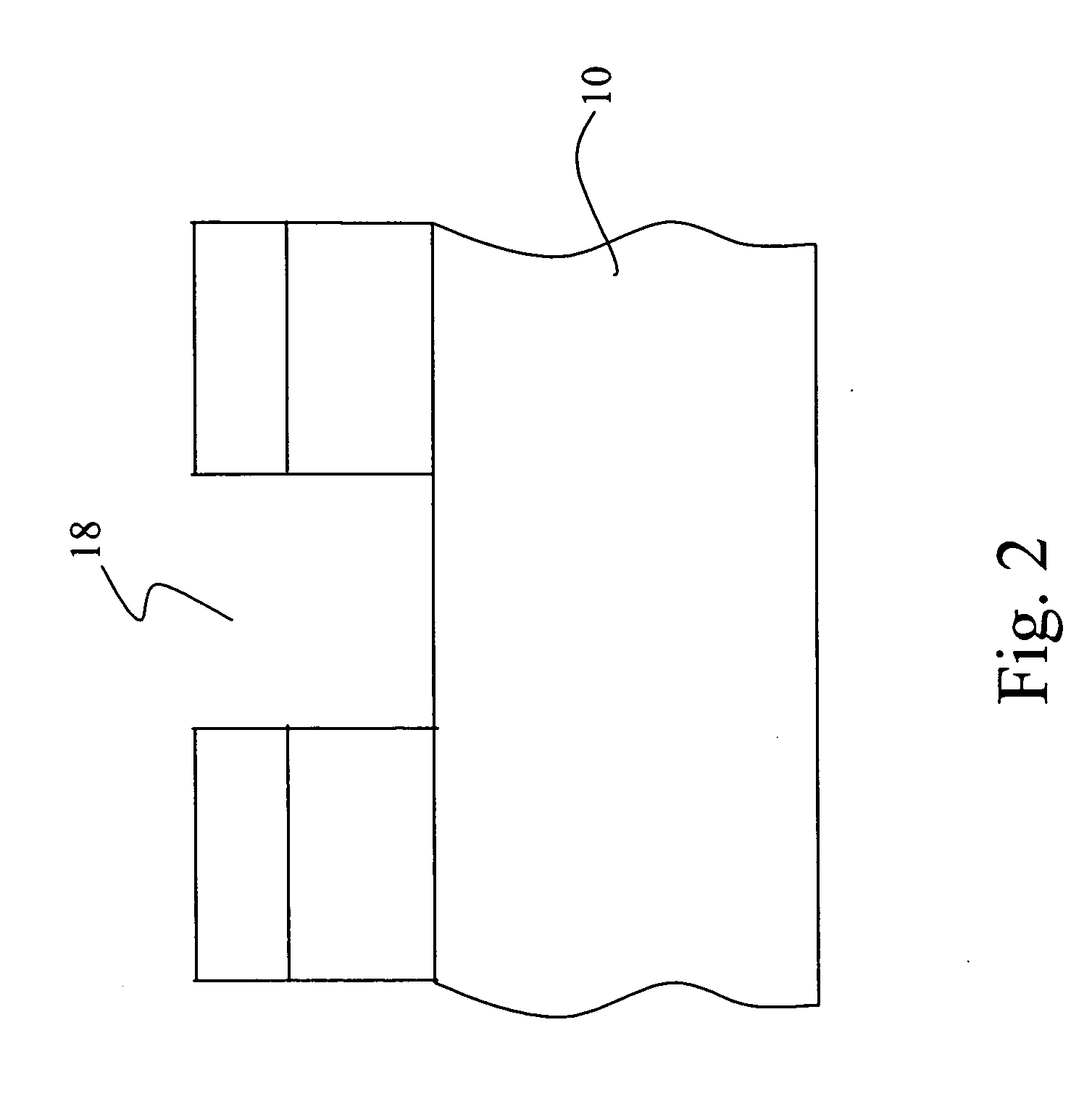
[0015] Refer to FIG. 1, a semiconductor substrate 10 having several isolation areas formed thereon is provided. An oxide layer 12, a hard mask layer 14, and a patterned first photoresist layer 16 in sequence are formed on the semiconductor substrate 10. The material of the hard mask layer 14 can be silicon oxynitride (SiOH) or tetraethyl-orthosilicate (TEOS) or other materials. The hard mask layer 14 is deposited by Low Pressure Chemical Vapor Deposition (LPCVD). Next, using the patterned first photoresist layer 16 as a mask, an etching process is performed on the hard mask layer 14 and the oxide layer 12 until the semiconductor substrate 10 is exposed, thereby forming a first trench 18. The patterned first photoresist layer 1...


PUM


Abstract

A method of fabricating a T-shaped polysilicon gate by using dual damascene process. An oxide layer, a hard mask layer, and a patterned first photoresist layer in sequence are formed on a semiconductor substrate. Using the patterned first photoresist layer as a mask, an etching process is performed on the hard mask layer to form a first trench. The patterned first photoresist layer is removed. An organic layer is then deposited in the first trench. A patterned second photresist layer is formed on the semiconductor substrate. Using the patterned second photresist layer as a mask, an etching process is performed on the hard mask layer to define a second trench dimension. The patterned second photoresist layer and the organic layer are removed. An oxide layer and a polysilicon layer are deposited in the first trench and the second trench. The residual hark mask layer is removed to obtain a T-shaped profile polysilicon gate.

Description

BACKGROUND OF THE INVENTION [0001] 1. Field of the Invention [0002] The present invention relates to a method of forming a T-shaped polysilicon gate, and more particularly, to a method of fabricating a T-shaped polysilicon gate by using dual damascene process. [0003] 2. Description of the Prior Art [0004] Many semiconductor devices and circuits are based on metal oxide semiconductor field effect transistors (MOSFETs). MOSFET device use the gate as a control gate. That is, the voltage signal of the gate controls the output performance. As semiconductor technology shrinks into the deep submicron region, devices have become more highly-integrated and reduced in dimension. When the source / drain junction of the transistor becomes a shallow junction, the main concerns about structure parameters are (1) the junction depth of the extension area, (2) the lateral length of the extension area, (3) the lateral doping concentration profile of the extension area and so on. Therefore, after the di...

Claims


Application Information

Patent Timeline
IPC IPC(8): H01L21/28H01L21/336
CPCH01L29/66583H01L21/28114
Inventor YEH, SHUANG-FENGCHEN, PIN-JENMA, HUI-PINGPAO, TA-YUNG
Owner GRACE SEMICON MFG CORP
Why Eureka
Try Eureka