Semiconductor device

a technology of semiconductors and devices, applied in the direction of pulse automatic control, pulse technique, electronic switching, etc., can solve the problems of steady current consumption and raise problems, and achieve the effect of easy execution

Inactive Publication Date: 2005-06-16
SOCIONEXT INC
View PDF8 Cites 13 Cited by
  • Summary
  • Abstract
  • Description
  • Claims
  • Application Information

AI Technical Summary

Benefits of technology

[0013] Within the range of the withstand voltage of the device and without steady current consumption, the first power-supply voltage or the second power-supply voltage is supplied to the high-side voltage-controlled device to put the high-side voltage-controlled device in an electrically conductive state or an electrically non-conductive state in accordance with the supplied voltage with the second power-supply voltage taken as a reference. In this way, electrical conduction of the high-side voltage-controlled device can be controlled.
[0014] Since the first and second voltage-controlled devices employed in the level conversion circuit have the same type of electrical conduction as the high-side voltage-controlled device, the control of the first and second power-supply voltages each appearing in the level conversion circuit as a floated voltage relative to the reference voltage can be executed with ease.
[0019] By supplying a voltage equal to or larger than the threshold voltage of a PMOS transistor between the gate and source of the transistor, the transistor can be put in an electrically conductive state. Since the second power-supply voltage is applied to the sources of the output, first and fourth PMOS transistors, by supplying a voltage with voltage drop equal to or larger than the threshold voltage from second power-supply voltage to the gates of the output, first and fourth PMOS transistors, the output, first and fourth PMOS transistors can be controlled to enter an electrically conductive state or an electrically non-conductive state provided that the first power-supply voltage and the second power-supply voltage are set at such values that the difference between the first and second power-supply voltages is equal to or larger than the threshold voltage of the output, first and fourth PMOS transistors. In addition, a circuit for supplying the first power-supply voltage and the second power-supply voltage to the output, second and fourth PMOS transistors can be constructed with ease by employing PMOS transistors suitable for execution of electrical conduction on voltages on the high side. Since such a circuit is composed of PMOS transistors, the level conversion circuit can be built with ease between the first and second power-supply voltages, which are voltages floating with respect to the reference voltage.

Problems solved by technology

In applications to a technical field of mainly portable devices required to operate at a low current consumption, such steady current consumption raises a problem.

Method used


Image

  • Semiconductor device
  • Semiconductor device
  • Semiconductor device

Examples


Embodiment Construction

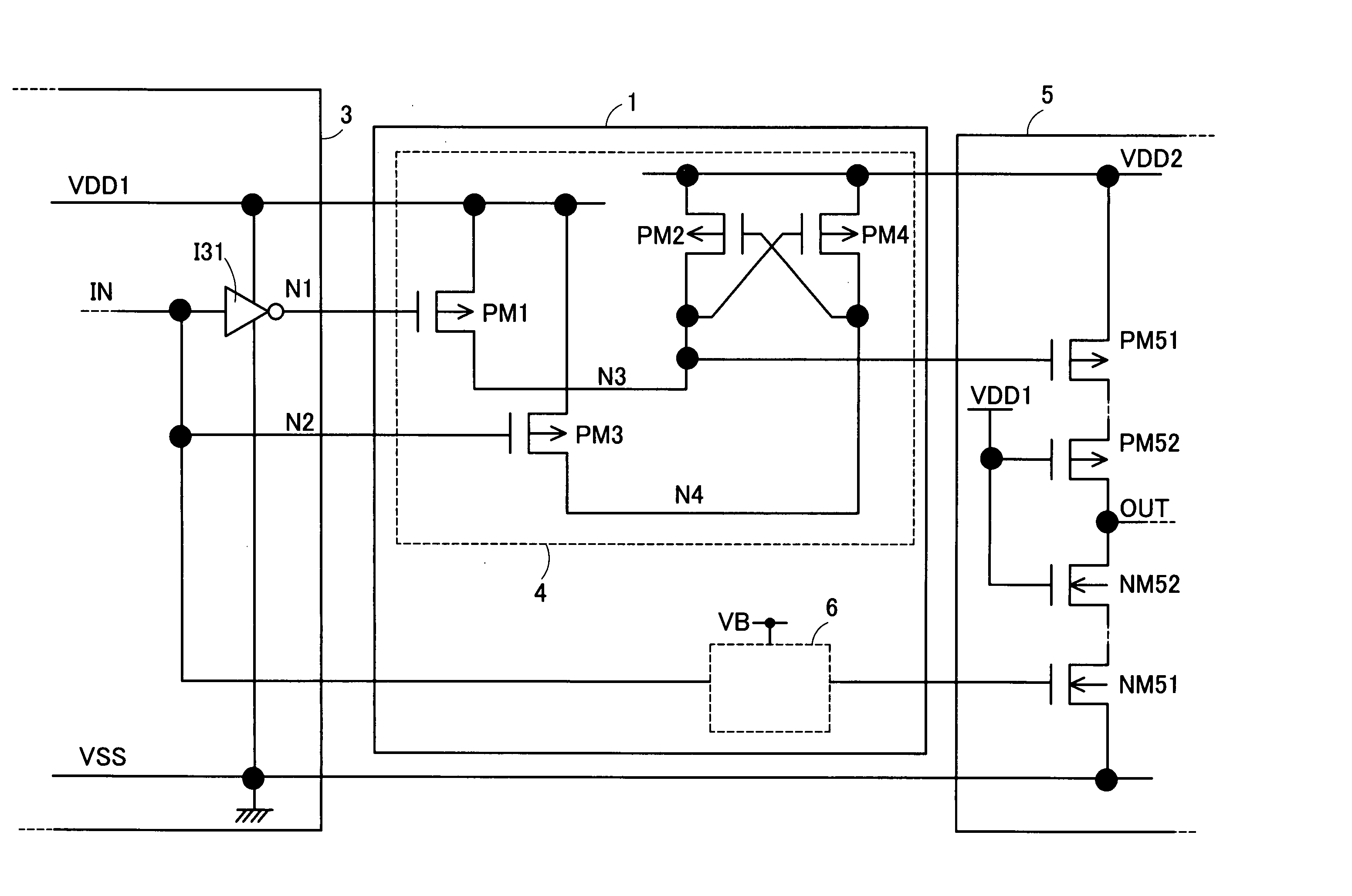
[0036] Embodiments implementing a semiconductor device provided by the present invention are explained by referring to FIGS. 1 to 14 as follows.

[0037]FIG. 1 is a circuit diagram showing a preferred embodiment implementing a semiconductor device provided by the present invention. The semiconductor device comprises a first circuit group 3 and a second circuit group 5. The first circuit group 3 is a group of circuits operating by being driven by a first power-supply voltage VDD1 relative to a reference voltage VSS. On the other hand, the second circuit group 5 is a group of circuits operating by being driven by a second power-supply voltage VDD2 relative to the reference voltage VSS. The second power-supply voltage VDD2 has a voltage level higher than the first power-supply voltage VDD1.

[0038] The first circuit group 3 is a circuit portion required to have a high processing speed. The first circuit group 3 is a circuit portion suitable for applications to control and processing, whic...


PUM


Abstract

In an operation to supply an input signal IN having an amplitude equal to a first power-supply voltage VDD1 to the gate of a PMOS transistor PM51 operating at a second power-supply voltage VDD2 higher than the first power-supply voltage VDD1, the levels of signals are converted by using PMOS transistors PM1 to PM4. The sources of the PMOS transistors PM1 and PM3 are connected to a line of the first power-supply voltage VDD1 whereas the sources of the PMOS transistors PM2 and PM4 are connected to a line of the second power-supply voltage VDD2. The gate of the PMOS transistor PM4 is connected to the drains of the PMOS transistors PM1 and PM2. The gate of the PMOS transistor PM2 is connected to the drains of the PMOS transistors PM3 and PM4. An inverted signal of the input signal IN is supplied to the gate of the PMOS transistor PM1 and the input signal IN is supplied to the gate of the PMOS transistor PM2. The amplitude of the input signal IN is converted from a magnitude equal to a difference between a reference signal VSS and the first power-supply voltage VDD1 into a magnitude equal to a difference between the first power-supply voltage VDD1 and the second power-supply voltage VDD2. A signal obtained as a result of the conversion is output from the PMOS transistors PM1 and PM2, being used for controlling electrical conduction of a PMOS transistor PM51.

Description

CROSS-REFERENCE TO RELATED APPLICATIONS [0001] This application is based upon and claims the benefit of priority from the prior PCT International Patent Application No. PCT / JP03 / 02178 filed on Feb. 27, 2003, the entire contents of which are incorporated herein by reference.BACKGROUND OF THE INVENTION [0002] 1. Field of the Invention [0003] The present invention relates to a semiconductor device having an interface for converting the level of a signal to a voltage level higher than the voltage of its own power supply. More particularly, the present invention relates to a semiconductor device capable of converting the level of a signal to a high voltage level without continuous current consumption. [0004] 2. Description of Related Art [0005] Japanese unexamined patent publication No. H10(1998)-22810 discloses an output buffer circuit capable of outputting a signal having a voltage level higher than the voltage of its own power supply. In accordance with the above publication '810, as ...

Claims


Application Information

Patent Timeline
Patent Type & Authority Applications(United States)
IPC IPC(8): H03K3/356H03K17/10H03K19/0185
CPCH03K17/102H03K3/356017
Inventor ITOH, KUNIHIRO
Owner SOCIONEXT INC
Why Eureka
Try Eureka