
Output circuit

a technology of output circuit and output waveform, which is applied in the field of output circuit, can solve the problems of low electric current consumption fine control, waveform distortion such as overshooting or undershooting of outputs, and can not be achieved, so as to reduce the electric current consumption of the operational amplifier, smooth output curve, and reduce the distortion of the output waveform of the operational amplifier.

Inactive Publication Date: 2005-06-16
RENESAS ELECTRONICS CORP
View PDF1 Cites 4 Cited by
  • Summary
  • Abstract
  • Description
  • Claims
  • Application Information

AI Technical Summary

Benefits of technology

[0013] An object of the present invention is therefore to provide an output circuit in which electric current consumption of operational amplifiers therein is reduced and distortion of the output waveforms of the operational amplifiers is also reduced.
[0025] According to the present invention, during the bias current control at the time of rise and fall of the output signals of the operational amplifiers, at the time of transition from the high biases to the low biases, the smooth output curves can be obtained. Electric current consumption of the operational amplifiers is thereby reduced and distortion of the output waveforms of the operational amplifiers can be reduced.

Problems solved by technology

For this reason, there is a problem that fine control for low electric current consumption cannot be performed.
Further, because of setting of the biases at the same high levels for the certain period of time, there is another problem that waveform distortion such as overshooting or undershooting of the outputs is apt to be generated.

Method used


Image

  • Output circuit
  • Output circuit
  • Output circuit

Examples


first embodiment

[First Embodiment]

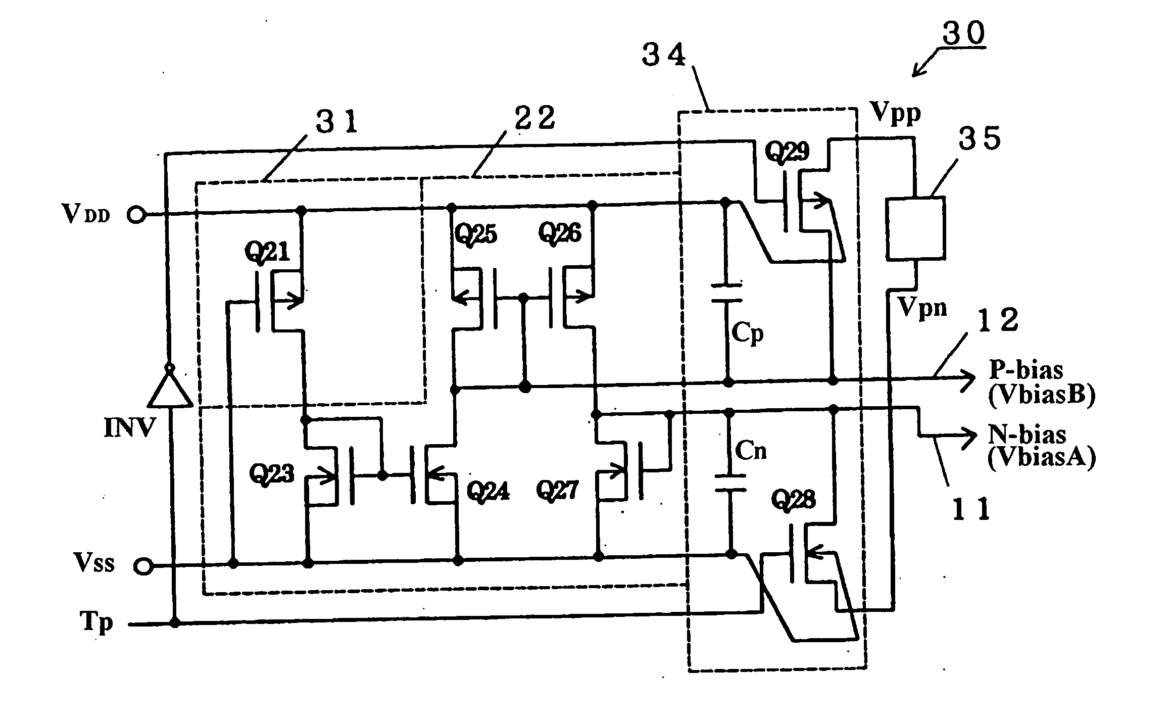
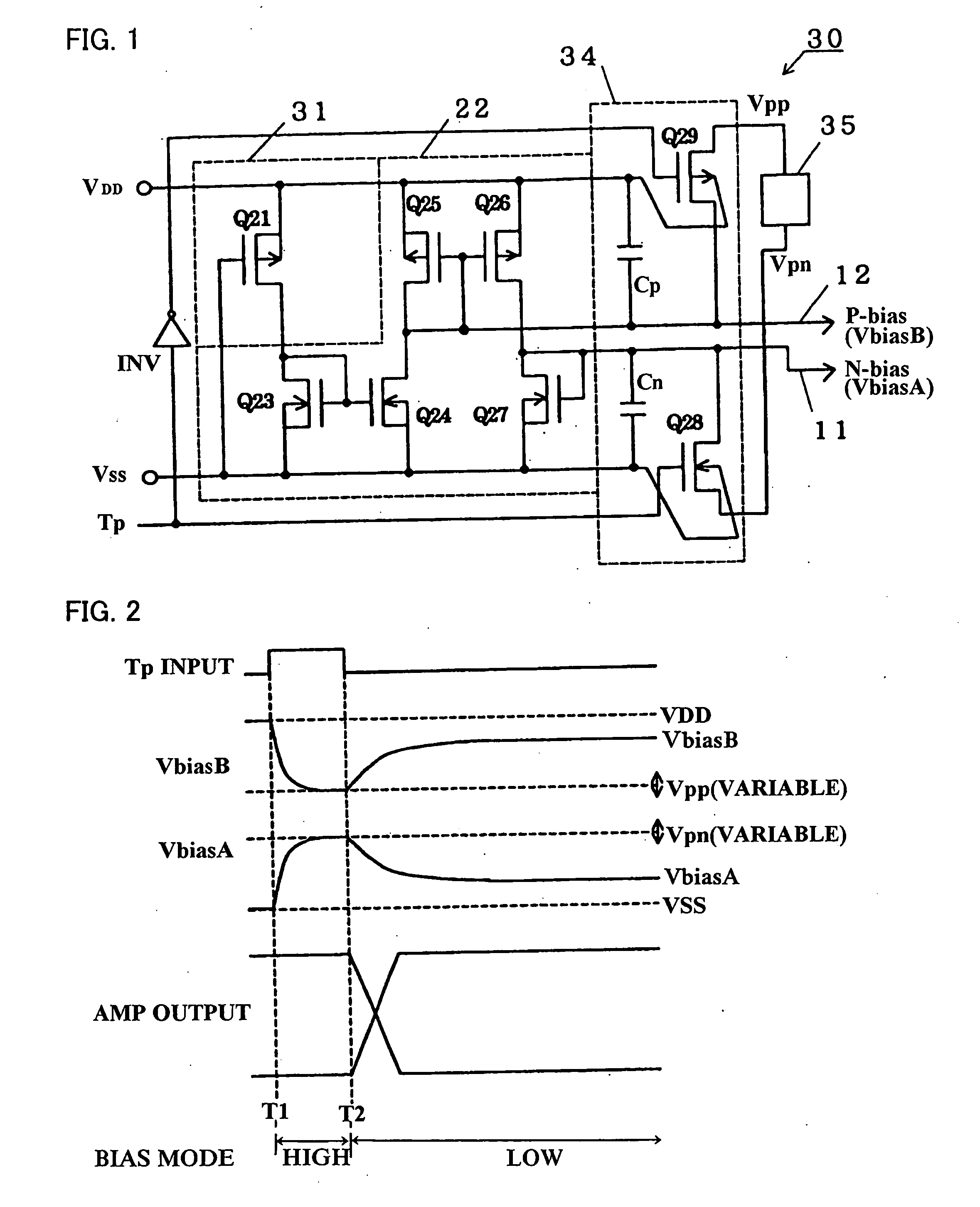
[0053] A bias circuit 30 according to a first embodiment to be used as a bias circuit 10 for output circuits 101 and 102 shown in FIGS. 7 and 10 will be described below with reference to FIG. 1, as an embodiment of an output circuit of the present invention. Incidentally, by assigning same reference characters to components having basic configurations that are the same as those shown in FIG. 12, their descriptions will be omitted. Its difference from a conventional bias circuit 20 shown in FIG. 12 is the presence of a bias current source 31 in place of a bias current source 21, and addition of a precharge circuit 34 and a precharge power supply 35. The bias current source 31 is different from the bias current source 21 in that an MOS transistor Q22 and an inverter 23 are eliminated therefrom and the bias current source 31 is made up of a MOS transistor Q21 so as to eliminate switching between high and low biases and make the bias current source 31 a bias current so...

second embodiment

[Second Embodiment]

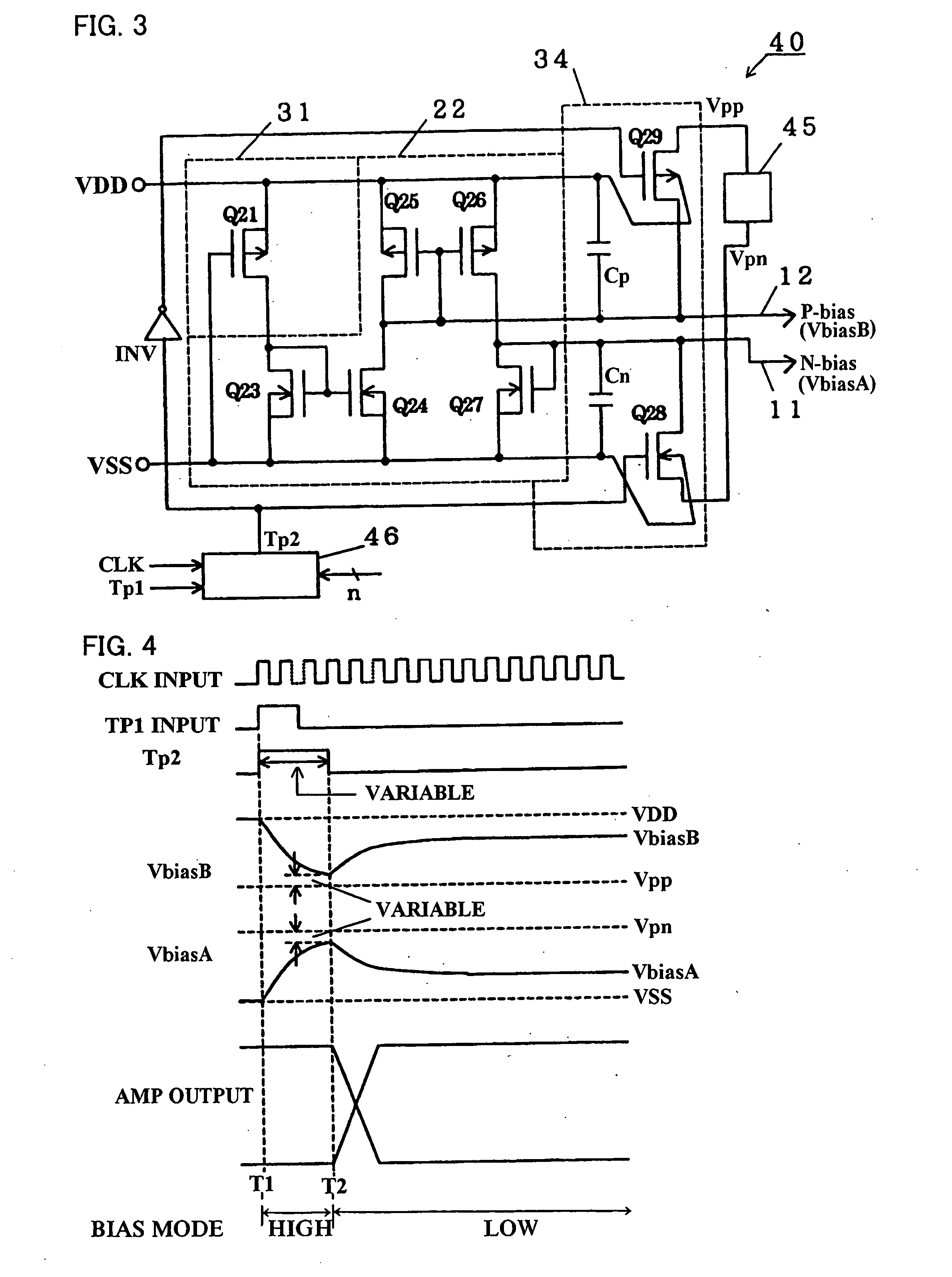
[0060] Next, a bias circuit 40 according to a second embodiment will be described with reference to FIG. 3. In FIG. 3, by assigning same reference characters to components that have same basic configurations as those shown in FIG. 1, their descriptions will be omitted. Its difference from the bias circuit 30 shown in FIG. 1 is the presence of a precharge power supply 45 in place of the precharge power supply 35 and addition of a pulse width adjusting circuit 46. Further, the precharge power supply 45 is different from the precharge power supply 35 in that the precharge power supply 45 is configured to output the precharge voltages Vpn and Vpp of predetermined constant voltages.

[0061] In the pulse width adjusting circuit 46, a desired n-bit count value is set. By counting its count value from rise of a timing signal Tp1 by a clock signal CLK, the pulse width adjusting circuit 46 outputs a timing signal Tp2 of a predetermined pulse width.

[0062] Next, an operation ...

third embodiment

[Third Embodiment]

[0065] Next, a bias circuit 50 according to a third embodiment will be described with reference to FIG. 5. In this embodiment, by assigning reference numerals to the components having basic configurations that are the same as those shown in FIG. 3, their description will be omitted. Its difference from the bias circuit 40 shown in FIG. 3 is the provision of a precharge circuit 54 in place of the precharge circuit 34 and no presence of the pulse width adjusting circuit 46. The precharge circuit 54 is different from the precharge circuit 34 in that the precharging capacitor Cn is connected between the low-voltage side terminal VSS and the series connection node between the MOS transistor Q26 and the MOS transistor Q27 via a variable resistance Rn, and that the precharging capacitor Cp is connected between the high-voltage side terminal VDD and the series connection node between the MOS via Q24 and the MOS transistor A25 via a variable resistance Rp.

[0066] When the b...


PUM

PropertyMeasurementUnit
precharge voltageaaaaaaaaaa
voltageaaaaaaaaaa
pulse widthaaaaaaaaaa

Abstract

Output circuit in which electric current consumption of operational amplifiers therein is reduced and distortion of the output waveforms of the operational amplifiers is also reduced. A bias circuit 30 is constituted from a bias current source 31, a bias voltage extracting circuit 22, a precharge circuit 34, and a precharge power supply 35. When a timing signal Tp of a predetermined pulse width is supplied to the bias circuit 30, MOS transistors 28 and 29 in the precharge circuit 34 are turned on during the period of its pulse width, and desired precharge voltages Vpn and Vpp are charged to capacitors Cn and Cp from the precharge power supply 35. The voltages charged to the capacitors Cn and Cp are supplied to operational amplifiers through an N-bias line 11 and a P-bias line 12 as bias voltages VbiasA and VbiasB, respectively, so that the operational amplifiers are controlled to be biased at high biases. The bias voltages VbiasA and VbiasB after precharging transition from high to low according to CR time constant curves for the discharge paths of the capacitors Cn and Cp. This transition period can be set by adjusting the precharge voltages using the variable precharge power supply 35.

Description

FIELD OF THE INVENTION [0001] The present invention relates to an output circuit. More specifically, the invention relates to an output circuit including operational amplifiers and a bias circuit for controlling the bias currents of the operational amplifiers so as to improve slew rates at the time of rise and fall of the output signals of the operational amplifiers. BACKGROUND OF THE INVENTION [0002] As a dot matrix type display device, liquid crystal display devices are employed for various devices such as a personal computer, because of its advantages of thinness, light weight, and low power consumption. Among them, color liquid crystal devices with an active matrix system which are particularly advantageous for controlling image quality with high definition, have become mainstream. In the liquid crystal display device of this type, an output circuit provided with operational amplifiers of a voltage follower connection and a bias circuit for controlling the bias currents of the o...

Claims


Application Information

Patent Timeline
Patent Type & Authority Applications(United States)
IPC IPC(8): G02F1/133G09G3/20G09G3/36H03F1/02H03F1/32H03F3/45H04N5/66
CPCH03F1/02H03F1/3211H03F3/45475H03F3/45237H03F3/45183
Inventor SEKO, YOSHIKAZU
Owner RENESAS ELECTRONICS CORP
Learn More