Patterned nanoscopic articles and methods of making the same

a patterned and patterned technology, applied in the direction of digital storage, instruments, semiconductor devices, etc., can solve the problems of increasing the density of fabrics, the inability to easily fabricate large-scale nanoscopic nanowire devices, and the decrease of resistance or enhancement of other conductive properties, so as to achieve the effect of enhancing resistance and enhancing properties

Active Publication Date: 2005-06-16
ZEON CORP
View PDF22 Cites 170 Cited by
  • Summary
  • Abstract
  • Description
  • Claims
  • Application Information

AI Technical Summary

Benefits of technology

[0039] According to one aspect of the invention, strapping materials are deposited on top of or through the nanowire fabrics to enhance their properties (e.g., addition of metals to the nanowire fabrics for stitching between devices to decrease resistance).

Problems solved by technology

Current technology does not allow for facile fabrication of large scale nanoscopic nanowire devices; there is therefore a need in the art for a method of creating structures of patterned nanowire fabrics.
For example, one application would result in a sparse fabric and multiple applications would result in increasingly dense fabric.
A denser fabric could lead to a decrease in resistance or enhancement of other conductive properties.

Method used


Image

  • Patterned nanoscopic articles and methods of making the same
  • Patterned nanoscopic articles and methods of making the same
  • Patterned nanoscopic articles and methods of making the same

Examples


Embodiment Construction

General

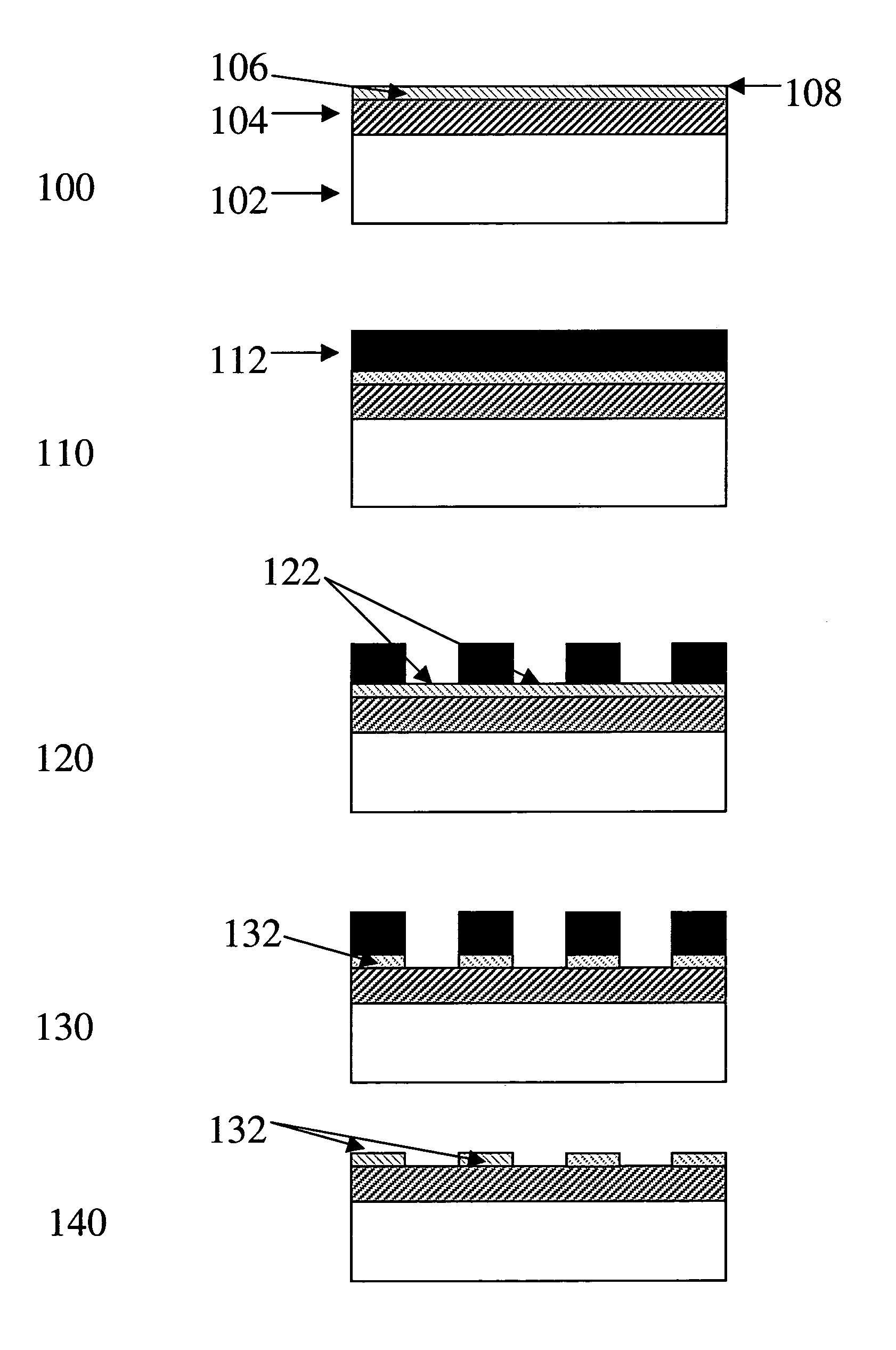
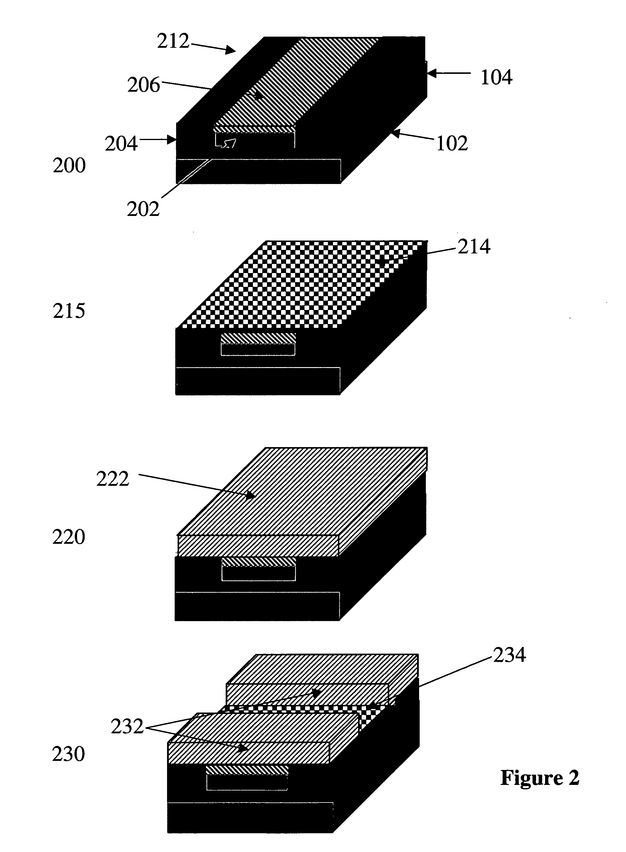
[0051] Methods for patterning nanoscale articles and nanoscale features are disclosed in which nanowires or a mixture of nanowires and nanotubes are placed on or grown onto a surface and defined into patterned articles.

Definitions

[0052] The term “nanowire” as used herein is meant to describe a nanoscale particle typically of high aspect ratio, regardless of the composition or electrical conductivity of the material.

[0053] The term “nanotube” or “nanotubes” as used herein is meant to mean carbon nanotubes. Carbon nanotubes may be pristine, functionalized, or they may be filled with other material, e.g., nanowire material.

[0054] The term “functionalization,” as used herein, includes both covalent and noncovalent modifications of nanotubes while the term “derivatization” signifies the covalent modification of nanotubes. Functionalization may in certain instances involve non-covalent transformation of the surface of a nanotube into a form with different functional groups or ...


PUM

PropertyMeasurementUnit
widthaaaaaaaaaa
diametersaaaaaaaaaa
widthaaaaaaaaaa

Abstract

Nanowire articles and methods of making the same are disclosed. A conductive article includes a plurality of inter-contacting nanowire segments that define a plurality of conductive pathways along the article. The nanowire segments may be semiconducting nanowires, metallic nanowires, nanotubes, single walled carbon nanotubes, multi-walled carbon nanotubes, or nanowires entangled with nanotubes. The various segments may have different lengths and may include segments having a length shorter than the length of the article. A strapping material may be positioned to contact a portion of the plurality of nanowire segments. The strapping material may be patterned to create the shape of a frame with an opening that exposes an area of the nanowire fabric. Such a strapping layer may also be used for making electrical contact to the nanowire fabric especially for electrical stitching to lower the overall resistance of the fabric.

Description

CROSS-REFERENCE TO RELATED APPLICATIONS [0001] This application claims the benefit under 35 U.S.C. § 119(e) of U.S. Provisional Patent Application No. 60 / 501,033, filed Sep. 8, 2003, and 60 / 503,099, filed Sep. 15, 2003, both entitled Patterning of Nanoscopic Articles, which are hereby incorporated by reference in their entirety. [0002] This application is related to the following references, which are assigned to the assignee of this application, and are hereby incorporated by reference in their entirety: [0003] Methods of Nanotube Films and Articles (U.S. patent application Ser. No. 10 / 128,117), filed on Apr. 23, 2002; and [0004] Non-Volatile Electromechanical Field Effect Devices and Circuits Using Same and Methods of Forming Same (U.S. patent application Ser. No. 10 / 864,186), filed on Jun. 9, 2004.BACKGROUND [0005] 1. Technical Field [0006] This invention relates in general to the patterning of nanoscopic materials, films, fabrics, layers, and articles and in particular to the pa...

Claims


Application Information

Patent Timeline
Patent Type & Authority Applications(United States)
IPC IPC(8): G11C11/00
CPCB82Y10/00H01L51/0023H01L51/0048H01L2924/0002Y10S977/762Y10S977/767Y10S977/856Y10S977/724H01L2924/00H10K71/621H10K85/221
Inventor SEGAL, BRENT M.RUECKES, THOMASBERTIN, CLAUDE L.
Owner ZEON CORP
Why Eureka
Try Eureka