Check patentability & draft patents in minutes with Patsnap Eureka AI!

Metalized dielectric substrates for EAS tags

a technology of dielectric substrates and metalized dielectric plates, applied in the field of metalized dielectric substrates, can solve the problems of consuming nearly 50% of the available surface area of large capacitor plates, and achieve the effects of reducing the surface area of tags, maximizing surface area, and improving reliability and the facility of the tag deactivation process

Inactive Publication Date: 2005-06-16
MICROMETAL TECH
View PDF22 Cites 3 Cited by
  • Summary
  • Abstract
  • Description
  • Claims
  • Application Information

AI Technical Summary

Benefits of technology

[0015] One of the objectives of the present invention is the provision of a technique and article by which the reliability and the facility of the tag deactivating process is improved. To that end, the present invention departs from conventional practice and the prior art in that a very thin layer of dielectric material containing a very small opening or so-called via hole is formed directly on a first layer of conductive foil and a second layer of very thin conductive metal is deposited on the dielectric layer and in the via hole to effect the interconnection of the two conductive layers. This substrate construction is subsequently patterned with an etch resist, and then etched to form the inductor and capacitor plates that constitute the elements of the resonant circuit. Unlike conventional practice, wherein the reliability of the tag deactivation process is compromised by the need to precisely deform a thin polymeric layer by mechanical means, the deactivation reliability of tag circuits made from this construction is enhanced by the uniformity and consistency with which the critical breakdown thickness of its dielectric layer is formed by non-mechanical means. The formation of the small via hole in the dielectric layer has a derivative benefit in that it also eliminates the need to devote tag surface area on the inductor side to the formation of a mechanical interconnect.
[0016] Another object of the present invention is the reduction of tag surface area that must be devoted to the capacitor plate on the inductor side so that the inductance of the coil, a property directed related to the square of the number of turns in the coil, can be maximized for any size tag but particularly for tags smaller than 1.5″ square. In conventional practice, the use of a 1 mil thick polymer dielectric layer produces a requirement for a capacitor plate and its attendant connections that can occupy nearly 10% of the overall area of a 1.5″ square tag. For 1″ square tag designs, which have only 40% of the area of the 1.5″ square tag to begin with, reliance on a 1 mil thick polymer dielectric layer leads to even larger capacitor plates that consume nearly 50% of the available surface area. These consequences are almost entirely eliminated in the present invention because the use of a very thin dielectric layer produces a requirement for a very small capacitor plate, one that is only a tiny fraction of the size of its conventional counterpart. The size of this tiny capacitor element is such that, regardless of its location relative to the inductor coil, it maximizes the surface area, hence number of coil turns that can be devoted to the layout of the inductor pattern. This inductance-enhancing feature can be exploited to increase the detection range of a given size tag or to produce smaller tags with the same detection range.

Problems solved by technology

For 1″ square tag designs, which have only 40% of the area of the 1.5″ square tag to begin with, reliance on a 1 mil thick polymer dielectric layer leads to even larger capacitor plates that consume nearly 50% of the available surface area.

Method used


Image

  • Metalized dielectric substrates for EAS tags
  • Metalized dielectric substrates for EAS tags
  • Metalized dielectric substrates for EAS tags

Examples


Embodiment Construction

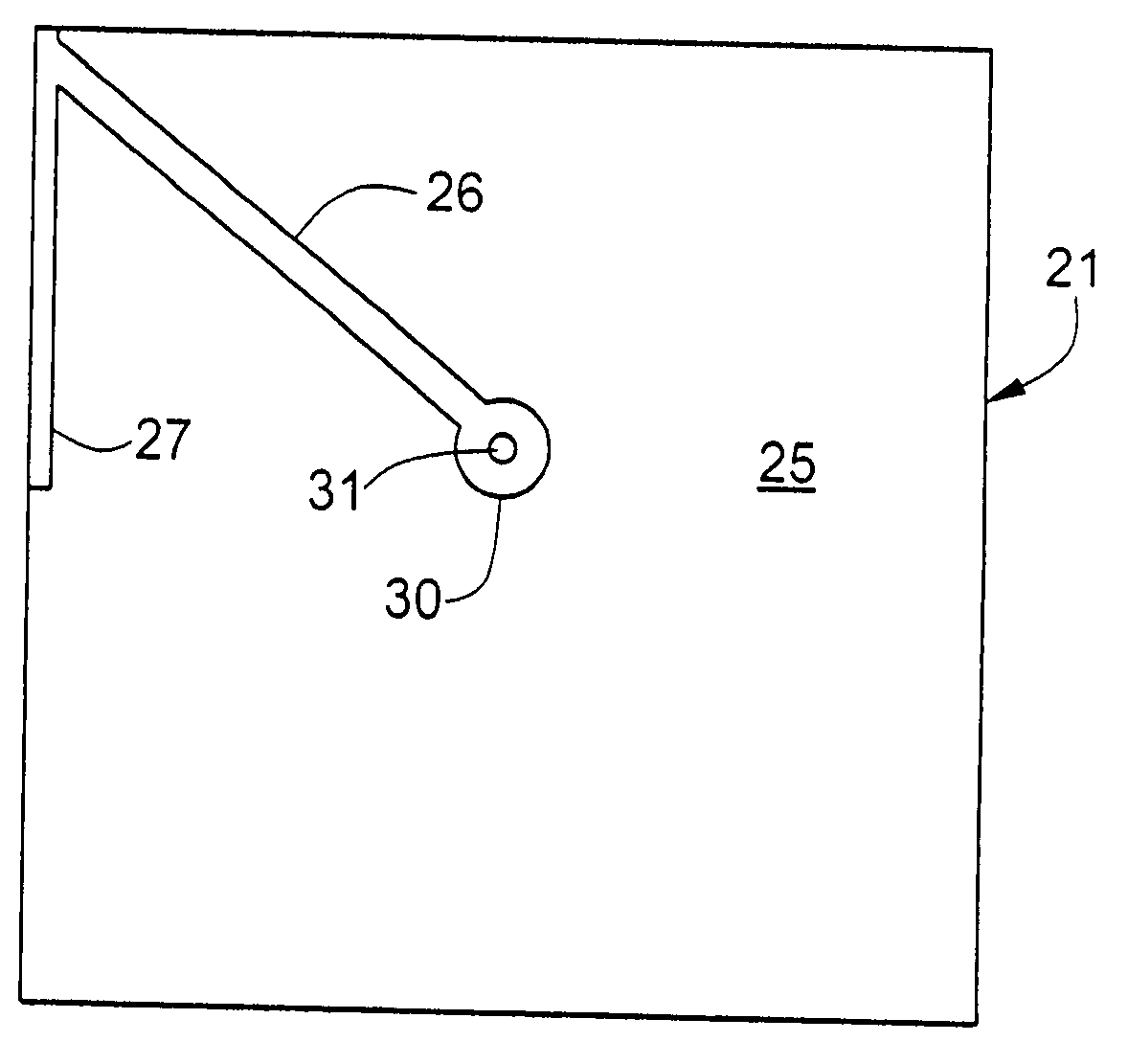
[0024]FIGS. 3A and 3B illustrate the features of a security tag 20 fabricated in accordance with the preferred embodiments of the present invention. As is well known in the art, the tag 20 is adapted to be secured on / in or otherwise borne by an article or item, or the packaging of such article, for which security or surveillance is sought. The tag 20 may be secured to the article or its packaging at a retail or other such facility, or as is often preferred, secured or incorporated into the article or its packaging by either the manufacturer or wholesaler of the article or a packaging specialist engaged by them. The tag 20 is employed in connection with an electronic article security system (not shown), particularly an electronic article security system of the radio frequency or RF type. Such electronic article security systems are well known in the art and therefore a complete description of the structure and operation of such electronic article security systems is not necessary for...


PUM

PropertyMeasurementUnit
thicknessaaaaaaaaaa
thickaaaaaaaaaa
thicknessaaaaaaaaaa

Abstract

A metallized substrate, such as used to make a resonant circuit tag with inductive and capacitive elements in series, has a thin inorganic or polymeric dielectric layer formed on a metal layer. The inorganic layer may be formed by anodizing a surface of the metal layer. The organic layer may be formed by flexographic printing. In both cases, a via hole is formed through the dielectric layer. A second layer of very thin conductive metal is deposited on the dielectric layer and in the via hole. The substrate is subsequently patterned with an etch resist and then etched to form the inductor coil and the capacitor plates, which are interconnected via the metallized via hole.

Description

CROSS REFERENCE TO RELATED APPLICATIONS [0001] This application is a continuation of U.S. application Ser. No. 10 / 137,195 filed May 2, 2002, and claims priority of U.S. Provisional Patent Applications Ser. No. 60 / 288,941 filed May 4, 2001 and Ser. No. 60 / 309,651 filed Aug. 2, 2001, the disclosures of which are incorporated by reference herein.STATEMENT REGARDING FEDERALLY SPONSORED RESEARCH OR DEVELOPMENT [0002] N / A FIELD OF THE INVENTION [0003] The present invention relates to metalized dielectric substrates and their utility in radio frequency electronic article surveillance tag circuits. BACKGROUND OF THE INVENTION [0004] The use of electronic article surveillance or security systems for detecting and preventing theft or unauthorized removal of articles or goods from retail establishments and / or other facilities, such as libraries, has become widespread. In general, such systems, sometimes called EAS systems, employ a label or security tag, also known as an EAS tag, that is affix...

Claims


Application Information

Patent Timeline
Patent Type & Authority Applications(United States)
IPC IPC(8): G08B13/24
CPCG08B13/2414
Inventor BURKE, THOMAS F.
Owner MICROMETAL TECH
Features
  • R&D
  • Intellectual Property
  • Life Sciences
  • Materials
  • Tech Scout
  • Unparalleled Data Quality
  • Higher Quality Content
  • 60% Fewer Hallucinations
Learn More