Triggererd back-to-back diodes for ESD protection in triple-well CMOS process
Inactive Publication Date: 2005-06-23
CHARTERED SEMICONDUCTOR MANUFACTURING
View PDF9 Cites 16 Cited by
Summary
Abstract
Description
Claims
Application Information
AI Technical Summary
This helps you quickly interpret patents by identifying the three key elements:
Problems solved by technology
Method used
Benefits of technology
[0023] The above and below advantages and features are of representative embodiments only, and are not exhaustive and/or exclusive. They are presented only to assist in understanding the invention. It should be understood that they are not representative of all the inventions defined by the claims, to be considered limitations on the invention as defined by the claims, or limitations on equivalents to the claims. For instance, some of these advantages may be mutually contradictory, in that they cannot be simultaneously present in a single embodiment. Similarly, some advantages
Problems solved by technology
However, current and foreseeable trends in the semiconductor industry are adversely impacting the effectiveness of known ESD circuits.
Designing ESD protection structures for high-speed analog and RF application is a challenge due to stringent requirement of input impedance and area.
The diode solution works fine except for the series resistance which results in voltage drop in the forward conduction mode.
In addition, current density of forw
Method used
Image
Click on the blue label to locate the original text in one second.
Reading with bidirectional positioning of images and text.
Examples
Example
First Example Embodiment of ESD Protection Device
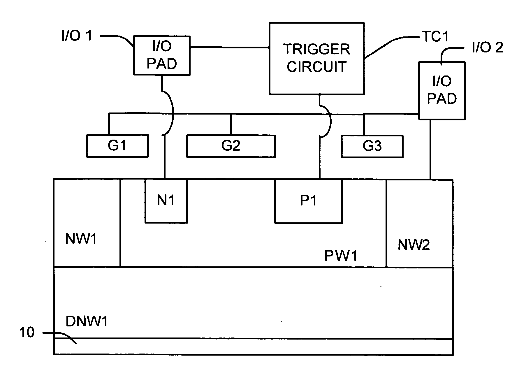
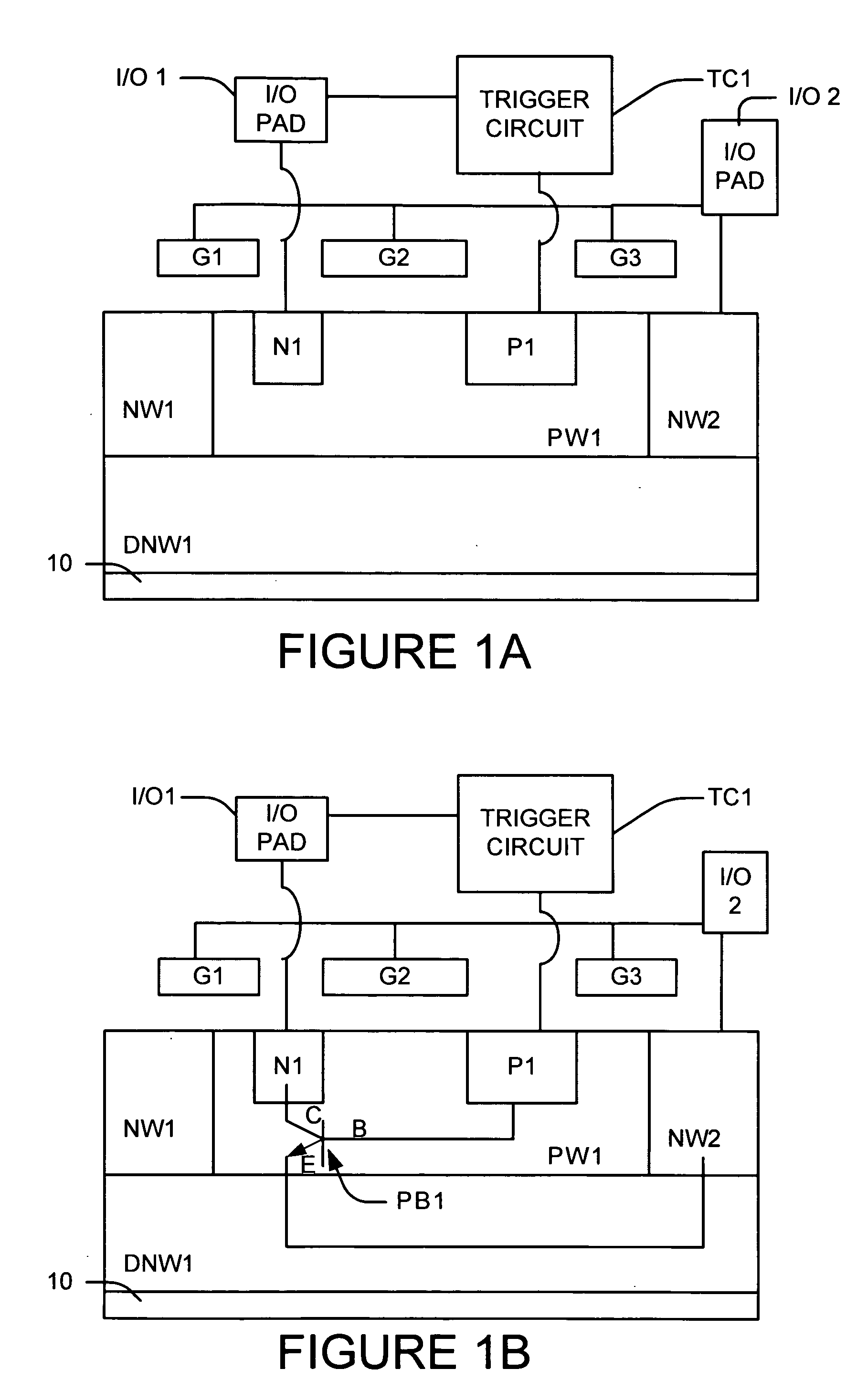
[0042] Referring to FIGS. 1A and 1B, a first example embodiment of ESD protection device is shown. FIG. 1B shows a representation of the a parasitic bipolar transistor (PB1). The example shows a first N doped region (N1), a p-well (PW1) and deep n-well (DNW1). But, the opposite conductivity type structure can be formed.
[0043] A substrate structure 10 is provided. The semiconductor structure can be comprised of silicon (Si). The top surface of the substrate structure 10 is preferably a p minus doped silicon layer, such as the top portion of a p type silicon wafer.
[0044] A n-doped region (N1) and a p-doped region (P1) are in a p-well (PW1) in a semiconductor structure 10. The n-doped region (N1) and a p-doped region (P1) are preferably spaced apart.
[0045] The n-doped region (N1) and a p-doped region (P1) are preferably spaced by the p-well (PW1).
[0046] The n-doped region (N1) and a p-doped region (P1) could be spaced by isolation ...
Example
[0057]FIG. 1C shows a top down view of an aspect of the first embodiment (See FIGS. 1A and 1B). The first gate (G1) is not shown as P1 completely surround N1 in this example layout. Also, the trigger circuit is not shown.
Operation of the ESD Device—parasitic Bipolar Transistor (PB1)
[0058] Referring to FIG. 1B, a (vertical) parasitic bipolar transistor (PB1) is comprised of the n-doped region (N1) functioning as a collector terminal, the P-well (PW1) functioning as a base terminal, and the deep N-well (DNW1) functioning as the emitter terminal.
Normal Conditions
[0059] The P-well is grounded under normal operation making back-to-back diode difficult (to impossible) to turn on and offer good leakage behavior.
ESD condition
[0060] Under an ESD condition, the p-well (PW1) is charged positive using the trigger circuit (TC1) and the parasitic bipolar transistor (PB1) can be turned on. An ESD condition can be a positive voltage to the I / O pad.
[0061] Normally, the deep well is coupled...
PUM
Abstract
An embodiment is a Electro Static Discharge (ESD) protection device comprising: a n-doped region and a p-doped region in a p-well in a semiconductor structure. The n-doped region and the p-doped region are spaced. A n-well and a deep n-well surrounding the p-well on the sides and bottom. A first I/O pad connected to the n-doped region. A trigger circuit connected the first I/O pad and the p-doped region. A second I/O pad connected to the n-well. A parasitic bipolar transistor is comprised of the n-doped region that functions as a collector terminal, the P-well that functions as a base terminal, and the deep N-well that functions as the emitter terminal. Whereby under an ESD condition, the p-well is charged positive using the trigger circuit and the parasitic bipolar transistor can be turned on.
Description
BACKGROUND OF INVENTION [0001] 1) Field of the Invention [0002] This invention relates generally to Electro Static Discharge (ESD) devices and methods thereof and more particularly to an electrostatic discharge method and device comprising a parasitic bipolar transistor and a deep well. [0003] 2) Description of the Prior Art [0004] In the semiconductor industry, the use of electrostatic discharge protection (ESD) devices is known. ESD circuits ensure that integrated semiconductor devices are not destroyed by static electricity during routine post-manufacture processes. However, current and foreseeable trends in the semiconductor industry are adversely impacting the effectiveness of known ESD circuits. [0005] Designing ESD protection structures for high-speed analog and RF application is a challenge due to stringent requirement of input impedance and area. Various techniques have been invented for extending the traditional ESD protection device in RF area. Most involve some form of d...
Claims
Application Information
Patent Timeline
Application Date:The date an application was filed.
Publication Date:The date a patent or application was officially published.
First Publication Date:The earliest publication date of a patent with the same application number.
Issue Date:Publication date of the patent grant document.
PCT Entry Date:The Entry date of PCT National Phase.
Estimated Expiry Date:The statutory expiry date of a patent right according to the Patent Law, and it is the longest term of protection that the patent right can achieve without the termination of the patent right due to other reasons(Term extension factor has been taken into account ).
Invalid Date:Actual expiry date is based on effective date or publication date of legal transaction data of invalid patent.
IPC IPC(8): H01L23/62H01L27/02
CPCH01L27/0259
Inventor MANNA, INDRAJLTLO, KENG FOOTAN, PEE YAFILIPPI, RAYMOND