Scanning electron microscope

a scanning electron microscope and scanning electron technology, applied in the field of scanning electron microscope, can solve the problems of deteriorating resolution of image shifting system employed in the conventional sem, economic infeasibility of mechanical control of the stage position in an accuracy of nanometers, and difficult in respect of moving speed

Inactive Publication Date: 2005-06-30
HITACHI LTD
View PDF28 Cites 9 Cited by
  • Summary
  • Abstract
  • Description
  • Claims
  • Application Information

AI Technical Summary

Benefits of technology

[0004] When a SEM is used for the inspection of a semiconductor device during semiconductor device fabricating processes or a completed semiconductor device, capability of rapidly moving an observation point to tens of inspection positions on a semiconductor wafer is a prerequisite of the SEM for the improvement of the throughput of an inspection process. Therefore, a stage capable of rapid movement has been used. However, the positioning accuracy of the stage is on the order of several micrometers. Mechanical control of the position of the stage in an accuracy on the order of nanometers is economically infeasible and is practically difficult in respect of moving speed. Therefore, to position the stage in a high accuracy higher than several micrometers, there is adopted an image shifting system that shifts electrically the coordinates of the scanning center of a primary electron beam. In some cases, since the coordinates are shifted by a distance as long as several micrometers, the image shifting system employed in the conventional SEM deteriorates resolution when the distance of shift is great.
[0005] According to the present invention it is an object of the present invention to provide a SEM capable of image shifting an image without causing significant deterioration of resolution.

Problems solved by technology

Mechanical control of the position of the stage in an accuracy on the order of nanometers is economically infeasible and is practically difficult in respect of moving speed.
In some cases, since the coordinates are shifted by a distance as long as several micrometers, the image shifting system employed in the conventional SEM deteriorates resolution when the distance of shift is great.

Method used


Image

  • Scanning electron microscope
  • Scanning electron microscope
  • Scanning electron microscope

Examples


first embodiment

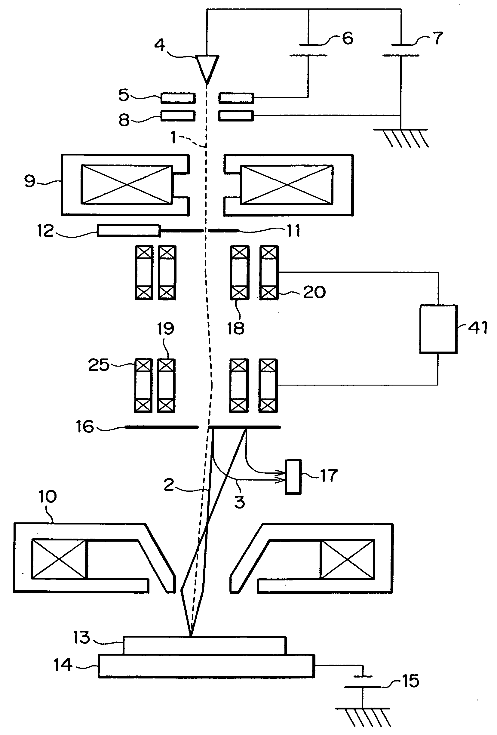
[0018]FIG. 1 shows a SEM in a first embodiment according to the present invention. A cathode 4 emits electrons when a beam voltage 6 is applied across the cathode 4 and an emission control electrode 5. The electrons thus emitted are accelerated (decelerated in some cases) by the emission control electrode 5 and an anode 8 held at a ground voltage. An acceleration voltage for accelerating a primary electron beam 1 is equal to an electron gun acceleration voltage 7. The primary electron beam 1 accelerated by the anode 8 is gathered by a condenser lens 9. Angle of divergence of the primary electron beam 1 or beam current is determined by a diaphragm 11 disposed below the condenser lens 9. A knob 12 is operated for centering the diaphragm 11.

[0019] The primary electron beam 1 having passed the diaphragm 11 is deflected by image shifting deflectors 20 and 30 having a scanning deflection function for image shifting, and is moved on a specimen 13 for two-dimensional scanning. The deflectin...

fourth embodiment

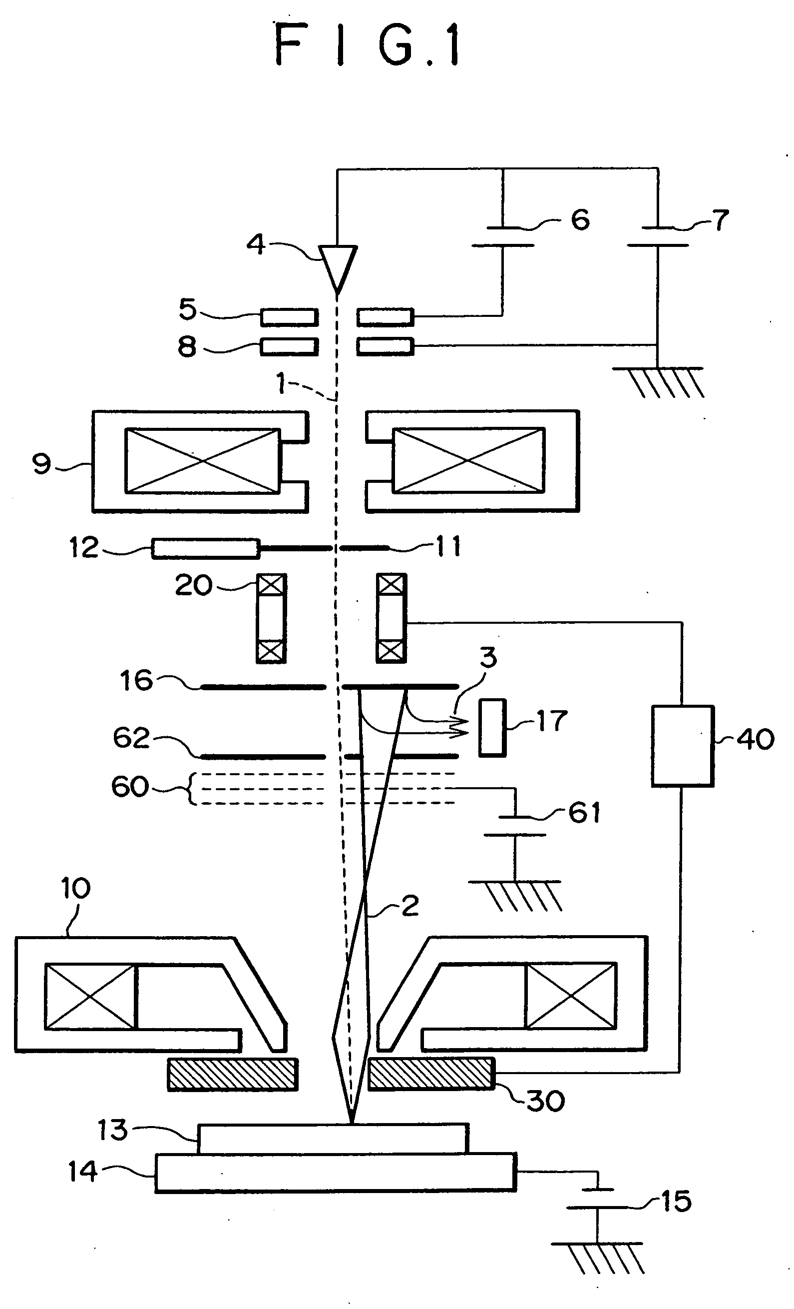
[0041]FIG. 11 is a view of assistance in explaining a SEM in a fourth embodiment according to the present invention. FIG. 11 shows typically a deflection range 101 for image shifting. The SEM as shown in FIG. 1 is provided with a controller, not shown. The controller sets values of parameters including observation positions and magnification, and controls a mirror included in the SEM on the basis of the set values. A SEM for inspecting semiconductor wafers needs to observe a plurality of points on the surface of a semiconductor wafer. Recipe specifying conditions for the observation of the plurality of points are set beforehand or the recipe is set manually.

[0042] A plurality of high-magnification observation regions 103 can be set in the deflection range 101 in which the electron beam is deflected by image shifting deflectors 20 and 30. As mentioned above, most secondary electrons from a central point 102 of the deflection range 101, i.e., a point corresponding to a primary electro...


PUM

PropertyMeasurementUnit
acceleration voltageaaaaaaaaaa
diameteraaaaaaaaaa
image shifting distanceaaaaaaaaaa

Abstract

The present invention is intended to prevent the deterioration of resolution due to increase in off-axis aberration resulting from the deviation of a primary electron bean from the optical axis of a scanning electron microscope. A scanning electron microscope is provided with an image shifting deflector system including two deflectors disposed respectively at upper and lower stages. The deflector disposed at the lower stage is a multipole electrostatic deflecting electrode and is disposed in an objective. Even if the distance of image shifting is great, an image of a high resolution can be formed and dimensions can be measured in a high accuracy. The SEM is able to achieving precision inspection at a high throughput when applied to inspection in semiconductor device fabricating processes that process a wafer having a large area and provided with very minute circuit elements.

Description

BACKGROUND OF THE INVENTION [0001] The present invention relates to a scanning electron microscope that scans the surface of a specimen with an electron beam and forms a two-dimensional electron image representing the shape or composition of the surface of the specimen through the detection of secondary signals produced by the specimen. More particularly, the present invention relates to a scanning electron beam microscope suitable for forming electron beam images of a high resolution at a high throughput by rapidly moving an observation point to tens of test positions on a semiconductor wafer as a specimen. [0002] A scanning electron microscope (hereinafter abbreviated to “SEM”) accelerates electrons emitted by an electron source of a heating electron emission type or a field electron emission type, collimates the accelerated electrons in a fine electron beam, i.e., a primary electron beam using an electrostatic lens or a magnetic field lens, scans a specimen two-dimensionally with...

Claims


Application Information

Patent Timeline
Patent Type & Authority Applications(United States)
IPC IPC(8): G21K7/00H01J37/147G01Q30/02H01J37/28
CPCH01J37/147H01J37/1471H01J37/153H01J37/28H01J2237/2817H01J2237/14H01J2237/1516H01J2237/244H01J2237/12
Inventor OSE, YOICHITODOKORO, HIDEOEZUMI, MAKOTOSATO, MITSUGU
Owner HITACHI LTD
Why Eureka
Try Eureka