Dicing die-bonding film

a die-bonding film and die-bonding technology, applied in film/foil adhesives, basic electric elements, semiconductor/solid-state device testing/measurement, etc., can solve the problems of inability to peel the portion which is stuck onto the dicing frame, the adhesive layer is not easily uniform, and the portion which is stuck onto the semiconductor wafer cannot be peeled. , to achieve the effect of easy peeling, easy peeling and picking up the resultant chip-form

Inactive Publication Date: 2005-06-30
NITTO DENKO CORP
View PDF18 Cites 69 Cited by
  • Summary
  • Abstract
  • Description
  • Claims
  • Application Information

AI Technical Summary

Benefits of technology

[0028] The pressure-sensitive adhesive layer (2) can be designed to have the portions (2a and 2b), which correspond to the work-attaching area (3a) of the die-bonding adhesive layer (3) and the area (3b) other than the area (3a), in such a manner that the adhesive force of the pressure-sensitive adhesive layer portion (2a) to the die-bonding adhesive layer (3) is smaller than that of the pressure-sensitive adhesive layer portion (2b) to the layer (3). In other words, the pressure-sensitive adhesive layer portion (2b) bonds to the adhesive layer (3) to an appropriate extent at the time of dicing or expanding, so that the pressure-sensitive adhesive layer (2) is not peeled from the adhesive layer (3). On the other hand, the pressure-sensitive adhesive layer portion (2a) makes easy peeling possible. Therefore, no dicing poorness is given to even a large-sized chip having a larger size than a size of 10 mm×10 mm. The obtained dicing die-bonding film is a dicing die-bonding film making it possible to easily peel and pick up the resultant chip-form work obtained after the dicing. As described above, the dicing die-bonding film (1) of the invention has a good balance between holding power at the time of dicing and other times and peelability at the time of picking-up.
[0029] In the case that the dicing die-bonding film of the invention has a structure satisfying the following relationship: the adhesive force of the work-attaching area (3a) of the die-bonding adhesive layer (3) to a work is larger than that of the work-attaching area (3a) to the pressure-sensitive adhesive layer portion (2a), the chip-form work obtained after the work is diced can easily be peeled from the pressure-sensitive adhesive layer portion (2a) in the state that the die-bonding adhesive layer (3) is attached to the chip-form work.
[0030] In the dicing die-bonding film, a portion of the area (3b) other than the work-attaching area (3a) can be made into a mount-frame-attaching area (3b′). In the case that the adhesive force of the mount-frame-attaching area (3b′) of the die-bonding adhesive layer (3) to a mount frame is smaller than that of the area (3b′) to the adhesive layer portion (2b′), the dicing die-bonding film has a good balance between holding power at the time of dicing and other times and peelability at the time of picking-up.
[0031] The dicing die-bonding film of the present invention can be made into a structure having the pressure-sensitive adhesive layer (2) on the supporting substrate (1) and the die-bonding adhesive layer (3) which is peelable formed as the work-attaching area (3a) on a portion of the pressure-sensitive adhesive layer (2). The pressure-sensitive adhesive layer (2) can be designed to have the portion (2a) which corresponds to the work-attaching area (3a) and the other portion (2b) in such a manner that the adhesive force of the pressure-sensitive adhesive layer portion (2a) is smaller than that of the pressure-sensitive adhesive layer portion (2b). In other words, the pressure-sensitive adhesive layer portion (2a) makes easy peeling possible. On the other hand, a wafer ring can be bonded to the pressure-sensitive adhesive layer portion (2b). This can be fixed thereto so that this is not peeled at the time of dicing or expanding. Therefore, no dicing poorness is given to even a large-sized chip having a larger size than a size of 10 mm×10 mm. The obtained dicing die-bonding film is a dicing die-bonding film making it possible to easily peel and pick up the resultant chip-form work obtained after the dicing. As described above, the dicing die-bonding film of the invention has a good balance between holding power at the time of dicing and other times and peelability at the time of picking-up.

Problems solved by technology

In this method, however, the adhesive layer is not easily made uniform and further an especial device or a long time is required for the application of the adhesive.
However, there remains a problem that the portion which is stuck onto the semiconductor wafer and the portion which is stuck onto the dicing frame cannot be peeled.

Method used


Image

  • Dicing die-bonding film
  • Dicing die-bonding film
  • Dicing die-bonding film

Examples


embodiment 1

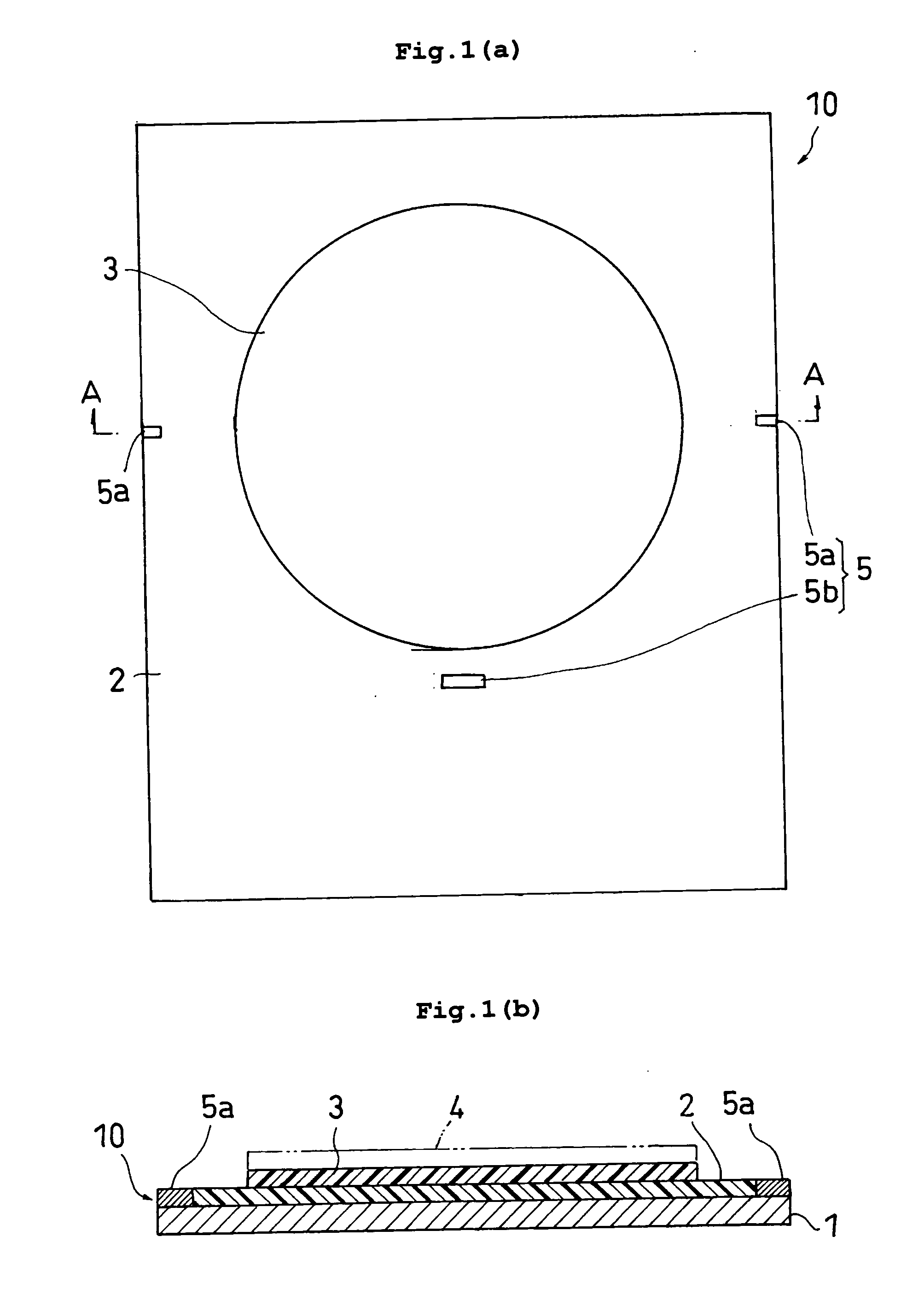
[0042] Embodiment 1 of the present invention is described hereinafter with reference to FIGS. 1(a) and 1(b). In the figures, however, parts or portions unnecessary for the description are omitted and some parts or portions are enlarged, scaled down or modified to make the description easy. The same matter is applied to the other drawings. FIG. 1(a) is a plan view of a dicing die-bonding film 10 according to the present embodiment, and FIG. 1(b) is a sectional view of the film taken on line A-A of FIG. 1(a), which is viewed along arrows.

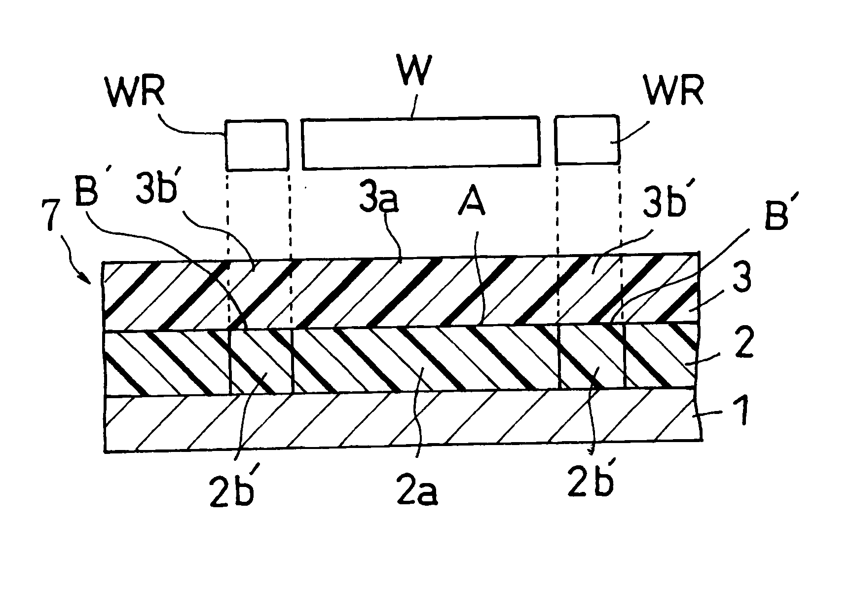
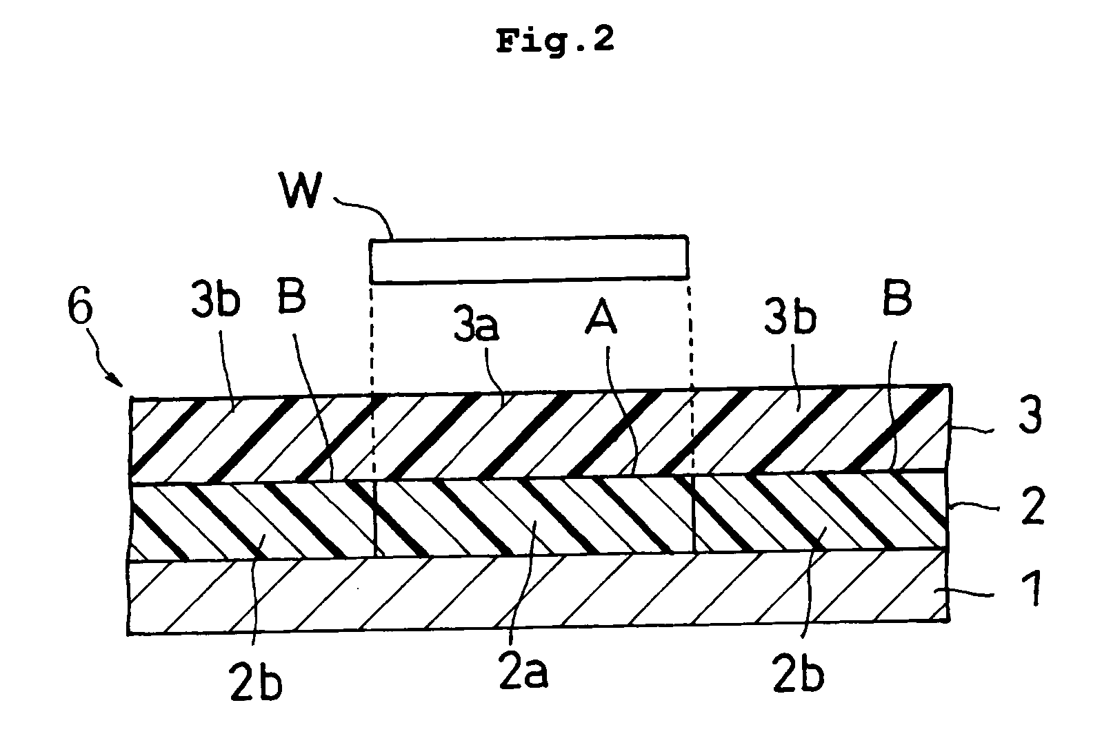
[0043] The dicing die-bonding film 10 of the present embodiment has a structure composed of a supporting substrate 1, a pressure-sensitive adhesive layer 2 formed on the supporting substrate 1, a die-bonding adhesive layer 3 formed on the pressure-sensitive adhesive layer 2, and position-recognizing marks for sticking the die-bonding adhesive layer 3 onto a semiconductor wafer (work) 4.

[0044] The supporting substrate 1 is a core member for giving st...

embodiment 2

[0099] In Embodiment 1, the case that colored layers made of ink or the like are used as the marks has been described. However, the present invention is not limited to this case. For example, an embodiment wherein only a given area of an adhesive layer is colored and the area is used as a mark can be adopted instead of the embodiment using the colored layer. FIG. 5 is a sectional view which schematically illustrates a dicing die-bonding film 11 according to the present embodiment.

[0100] An adhesive layer 12 in the present embodiment is a layer wherein a compound capable of being colored by irradiation with radial rays is incorporated into the adhesive layer 12 in Embodiment 1, and is irradiated through a photo-mask 13 having a given pattern with radial rays, whereby only a given area of the adhesive layer 12 is irradiated. In this way, only the area irradiated is colored to make it possible to form marks 12a, in a self-alignment manner, correspondingly to the pattern of the photo-m...

embodiment 3

[0110] The present embodiment is different from Embodiment 1 in that a marking adhesive film is used instead of the colored layer as the marks. The present embodiment is described hereinafter. FIG. 6 is a plane view which schematically illustrates a dicing die-bonding film 20 in the case that a marking adhesive film 21 is used.

[0111] The marking adhesive film 21 in the present embodiment 3 is made of an adhesive film. The material of the marking adhesive film 21 may be, for example, a colored polyolefin type adhesive tape. The thickness of the film marking adhesive 21 is not particularly limited, and is preferably from, e.g., 5 to 200 μm.

[0112] The position where the marking adhesive film 21 is formed is on any portion of a pressure-sensitive adhesive layer 2 except the portion where a die-bonding adhesive layer 3 is formed, the rear face of a supporting substrate 1, or between the supporting substrate 1 and the pressure-sensitive adhesive layer 2. The planer shape thereof is a re...


PUM

PropertyMeasurementUnit
sizeaaaaaaaaaa
thicknessaaaaaaaaaa
thicknessaaaaaaaaaa

Abstract

A dicing die-bonding film has a supporting substrate, an adhesive layer formed on the supporting substrate, and a die-bonding adhesive layer formed on the adhesive layer, and further has a mark for recognizing the position of the die-bonding adhesive layer. It is possible to provide a dicing die-bonding film in which in the case a semiconductor wafer and the dicing die-bonding film are stuck onto each other, the position of the die-bonding adhesive layer in the film can be recognized.

Description

FIELD OF THE INVENTION [0001] The present invention relates to a dicing die-bonding film for supplying, to the dicing of a work (such as a semiconductor wafer), an adhesive for fixing a chip-form work (such as a semiconductor chip) and an electrode member to each other in the state that the adhesive is attached to the work before the dicing. The present invention also relates to a method for fixing a chip-form work, using the dicing die-bonding film, and further relates to a semiconductor device to which a chip-form work is bonded and fixed by this fixing method. BACKGROUND OF THE INVENTION [0002] A semiconductor wafer wherein a circuit pattern is formed is adjusted into an appropriate thickness by polishing the rear face thereof if necessary, and then the wafer is diced into chips (the dicing step). In order to remove the resultant cut layer in this step, the semiconductor wafer is generally washed with a liquid in which an appropriate fluid pressure (usually, about 2 kg / cm2) is gi...

Claims


Application Information

Patent Timeline
Patent Type & Authority Applications(United States)
IPC IPC(8): C09J7/02C09J201/00H01L21/301H01L21/52H01L21/58H01L21/66H01L21/68H01L23/544
CPCH01L21/6836H01L22/20H01L2924/0665H01L2924/01006H01L2224/2919H01L2223/54426H01L23/544H01L24/27H01L24/83H01L2221/68327H01L2223/5442H01L2223/54453H01L2224/274H01L2224/83191H01L2224/8385H01L2924/01005H01L2924/01013H01L2924/01015H01L2924/01016H01L2924/01027H01L2924/01029H01L2924/01033H01L2924/01047H01L2924/01074H01L2924/01079H01L2924/01082H01L2924/014H01L2924/07802H01L2924/19043H01L2924/3025H01L24/29H01L2924/00H01L21/30
Inventor MATSUMURA, TAKESHIYAMAMOTO, MASAYUKI
Owner NITTO DENKO CORP
Why Eureka
Try Eureka