Method of manufacturing a semiconductor device

a manufacturing method and semiconductor technology, applied in semiconductor/solid-state device testing/measurement, semiconductor/solid-state device details, instruments, etc., can solve the problems of protection film peeling, drop in test efficiency and accordingly test reliability, and achieve the effect of improving the reliability of electrical inspection including burn-in test and functional testing, preventing chipping, and easing contact resistan

Active Publication Date: 2005-06-30
RENESAS ELECTRONICS CORP
View PDF12 Cites 24 Cited by
  • Summary
  • Abstract
  • Description
  • Claims
  • Application Information

AI Technical Summary

Benefits of technology

[0021] In a wafer level CSP or a bare chip, the formation of an inclined surface obliquely continuing to the main surface on the periphery of the main surface of the semiconductor chip by bevel cutting serves to ease the contact resistance which arises when the inclined surface comes into contact with the concave portion of a socket at the time of its insertion into the socket during electrical inspection. In addition, the absence of any edge part on the periphery of the main surface of the semiconductor chip can serve to prevent chipping which would otherwise occur when the semiconductor chip is inserted into the socket. As this makes it possible to prevent any silicon piece from remaining in the concave portion of the socket, the reliability of electrical inspection including the burn-in test and the functional test can be improved.

Problems solved by technology

If any of the chipped silicon pieces remains in the concave portion of the socket, there will arise a problem that the protective film over the surface of the semiconductor chip is damaged when the back surface of the semiconductor chip is pressed by the arm at the time of testing, eventually causing the protective film to be peeled off.
Furthermore, if any silicon piece remains in the concave portion of the socket, there will arise another problem that contact failure occurs between the protruding electrodes of the package and the terminals of the socket, inviting a drop in test efficiency and accordingly in test reliability.

Method used


Image

  • Method of manufacturing a semiconductor device
  • Method of manufacturing a semiconductor device
  • Method of manufacturing a semiconductor device

Examples


embodiment 1

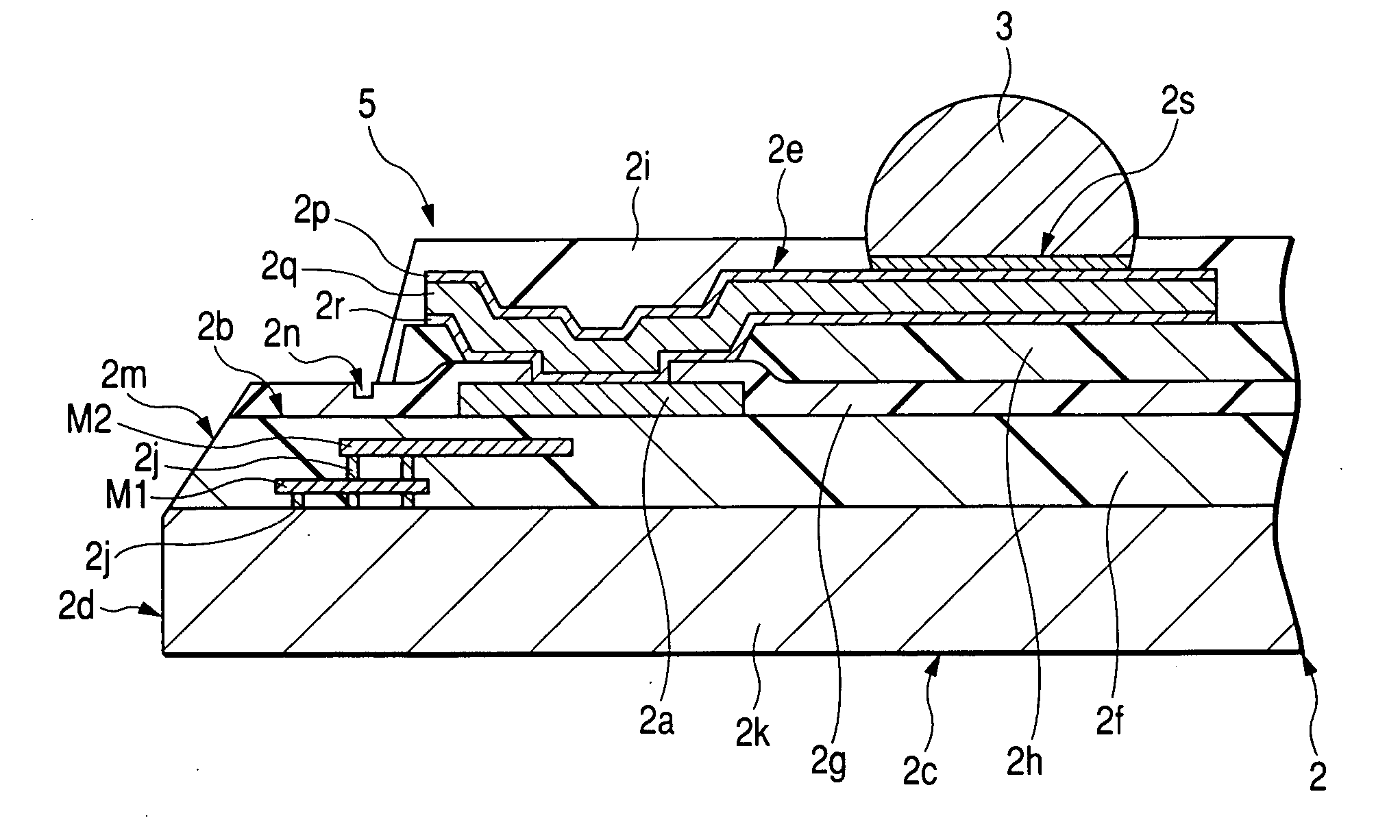
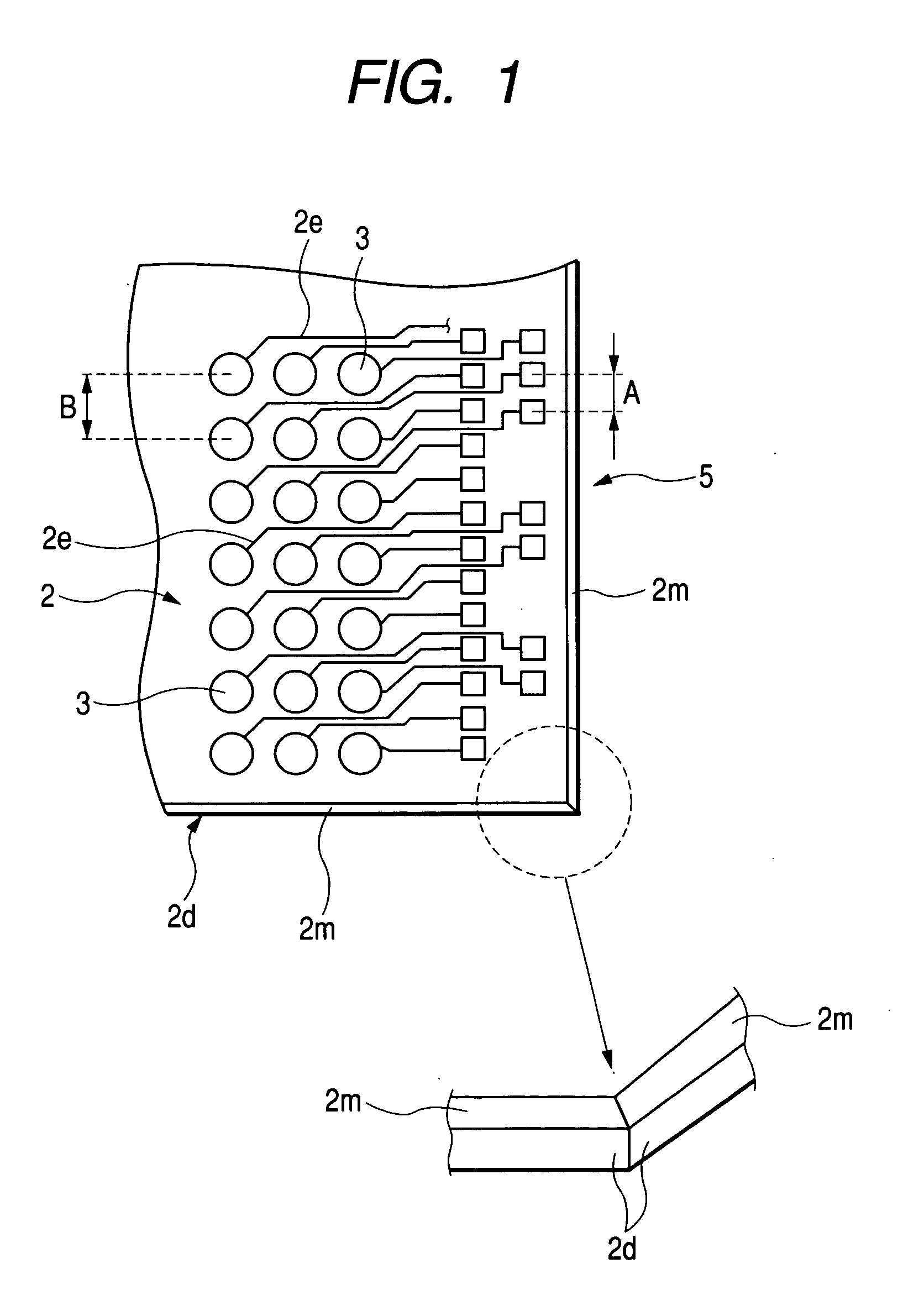
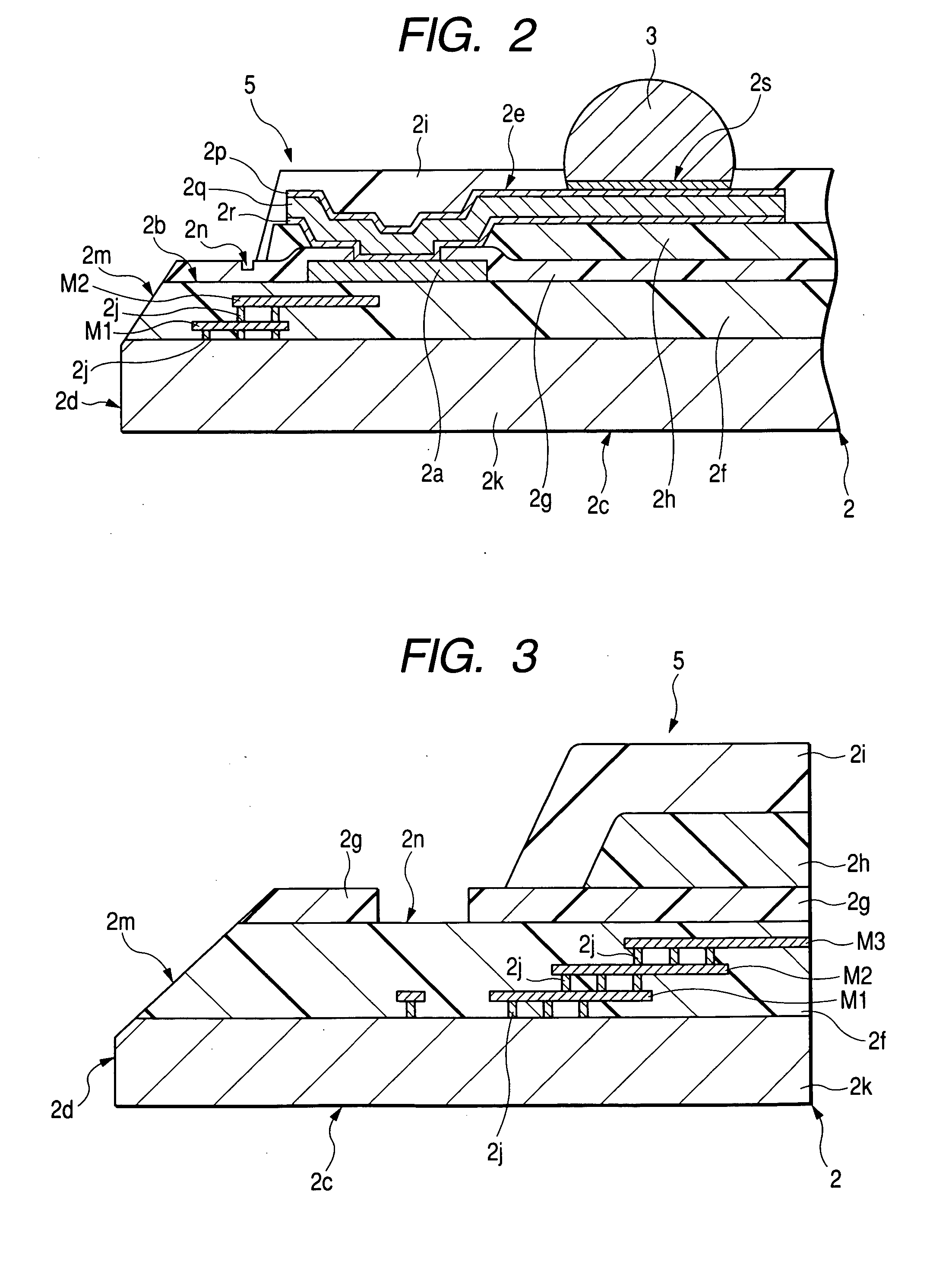
[0046]FIG. 1 consists of a partial plan showing one example of structure of a semiconductor device, which is Embodiment 1 of the invention, and an enlarged partial perspective view of a corner part thereof; FIG. 2 is an enlarged partial perspective view of one example of structure of the semiconductor device shown in FIG. 1; FIG. 3 is an enlarged partial section of the structure near an end of the semiconductor device shown in FIG. 1; FIG. 4 is a process flowchart of one example of procedure in the post-process of assembly of the semiconductor device shown in FIG. 1; FIG. 5 is an enlarged partial plan of one example of structure of a semiconductor wafer cut at the dicing step of assembly charted in FIG. 4; FIG. 6 is an enlarged partial section of the structure of the semiconductor wafer shown in FIG. 5; FIG. 7 is an enlarged partial section of one example of structure of the semiconductor wafer before bevel cutting at the dicing step charted in FIG. 4; FIG. 8 is an enlarged partial ...

embodiment 2

[0096]FIG. 20 is a section of one example of structure of a semiconductor device, which is Embodiment 2 of the present invention.

[0097] The semiconductor device of this Embodiment 2 shown in FIG. 20 comprises a bare chip 13 having a semiconductor element over its main surface 13a and solder bumps 3, which are a plurality of protruding electrodes disposed over that main surface 13a. An insulating film 13c is formed over a silicon substrate 13b, pads 13e, which are a plurality of electrodes, are formed over the main surface 13a of this insulating film 13c, and the solder bumps 3 are connected to the pads 13e via a barrier metal layer 13f.

[0098] Incidentally, in the bare chip 13, metal wiring is formed within the layer of the insulating film 13c, and a bevel cut surface 13g is formed to obliquely cross part or the whole, in the thickness direction, of this layer of the insulating film 13c.

[0099] Thus, when dicing the semiconductor wafer 1 (see FIG. 5) to form the bare chip 13, by us...


PUM


Abstract

Chipping of semiconductor chips is to be prevented. A semiconductor device comprises a semiconductor chip having a main surface, a plurality of pads formed over the main surface, a rearrangement wiring formed over the main surface to alter an arrangement of the plurality of pads, and a protective film and an insulating film formed over the main surface, and a plurality of solder bumps each connected to the rearrangement wiring and arranged differently from the plurality of pads. The presence of a bevel cut surface obliquely continuous to the main surface and formed on a periphery of the main surface of the semiconductor chip prevents chipping.

Description

CROSS-REFERENCE TO RELATED APPLICATION [0001] The present application claims priority from Japanese patent application No. 2003-433603 filed on Dec. 26, 2003, the content of which is hereby incorporated by reference into this application. BACKGROUND OF THE INVENTION [0002] The present invention relates to a semiconductor device and its manufacturing method, and more particularly to a technique that can be effectively applied to the prevention of chipping of semiconductor chips. [0003] In a semiconductor device of a conventional chip size, a semiconductor chip has a configuration mainly consisting of a semiconductor substrate and, formed over the circuit formation surface which is the outer of the inner and outer surfaces of this semiconductor substrate, a multi-layered wiring layer formed by stacking a plurality each of insulating layers and wiring layers, and a surface protecting film so formed as to cover this multi-layered wiring layer (see Patent Reference 1 for example). [0004]...

Claims


Application Information

Patent Timeline
Patent Type & Authority Applications(United States)
IPC IPC(8): G01R1/04G01R31/28G01R31/26G01R31/30H01L21/02H01L21/28H01L21/301H01L21/60H01L21/66H01L21/768H01L21/78H01L23/12H01L23/31H01L23/48H01L23/50H01L23/52H01L23/58H01L29/06
CPCG01R1/0483G01R31/2863H01L2924/0002H01L2924/00014H01L2224/0401H01L2924/10253H01L2224/05572G01R31/2886H01L21/78H01L23/3114H01L23/585H01L29/0657H01L2224/16H01L2924/01079H01L2224/05569H01L23/3171H01L2224/13022H01L2924/00H01L2224/05552H01L23/52H01L22/00
Inventor TAKAHASHI, NORIYUKI
Owner RENESAS ELECTRONICS CORP
Why Eureka
Try Eureka