Wireless IC tag, and method and apparatus for manufacturing the same

a technology of ic tags and wires, applied in the direction of insulated conductors, cables, instruments, etc., can solve the problems of short detectable distance, weak radio wave to be transmitted from the wireless tag, and absorbed radio wave in the metallic article of the wireless tag, so as to reduce durability, increase communication distance, and reduce the effect of durability

Inactive Publication Date: 2005-06-30
HITACHI LTD
View PDF7 Cites 215 Cited by
  • Summary
  • Abstract
  • Description
  • Claims
  • Application Information

AI Technical Summary

Benefits of technology

[0009] When the spacer thickness is increased in this manner, the communication distance can be increased. However, when the spacer thickness is increased to obtain a long communication distance, involves a large-sized wireless IC tag results. As a result, its application field is limited, thus being a hindrance. Even when such a large tag is actually used, the tag may be possibly peeled off due to contact with the person or object that it contacts, thereby reducing durability.
[0010] Even when such a tag is mounted to a cable, the communication distance of the tag is remarkably reduced, because the interior of the cable may be a metallic conductor such as copper or a metallic shield layer may be applied to the inside of an outer layer thereof. Further, when the wireless IC tag is bonded and mounted onto the surface of the cable, the tag may be easily dismounted. In addition, when the wireless IC tag is buried in the interior of the cable, the substrate of the tag cannot withstand the high temperature encountered when the cable is molded. In this way, the durability of the wireless IC tag is still a problem.
[0011] The present invention solves this problem. It is an object of the present invention to provide a wireless IC tag which can have a small thickness and a long communication distance even when mounted in the vicinity of a metallic part and which is less likely to be dismounted or destroyed by a high temperature even when mounted to a cable or the like, and also to provide a method and apparatus for manufacturing the wireless IC tag.
[0012] In order to solve the aforementioned problem, a wireless IC tag in accordance with the present invention includes a first antenna and a first spacer. The tag produces an operating power from a radio wave having a predetermined frequency and received at the first antenna to operate an IC chip, and reads out and transmits identification information stored in the chip. The tag also includes a second antenna having a predetermined length and having an auxiliary function of resonating to a radio wave having a predetermined frequency and strengthening an radio wave to be transmitted from the first antenna, and a second spacer disposed between the first and second antennas for maintaining a distance between both antennas.

Problems solved by technology

The aforementioned wireless tag, however, has a problem that, when the wireless tag is bonded to a metallic article, a radio wave received by the wireless tag is absorbed in the metallic article.
Thus, the intensity of radio wave to be transmitted from the wireless tag becomes weak and thus its detectable distance becomes short.
This problem similarly arises even in a wireless IC tag having an IC chip added thereto.
Thus, the tag cannot obtain a sufficient operating power.
This eventually results in the tag not being able to operate the IC chip to read the information, nor transmit the information a sufficiently far enough distance.
Since the thick spacer leads to an increase in the size of the wireless IC tag (an increase in the thickness in this example), this method cannot be easily employed.

Method used


Image

  • Wireless IC tag, and method and apparatus for manufacturing the same
  • Wireless IC tag, and method and apparatus for manufacturing the same
  • Wireless IC tag, and method and apparatus for manufacturing the same

Examples


embodiment 1

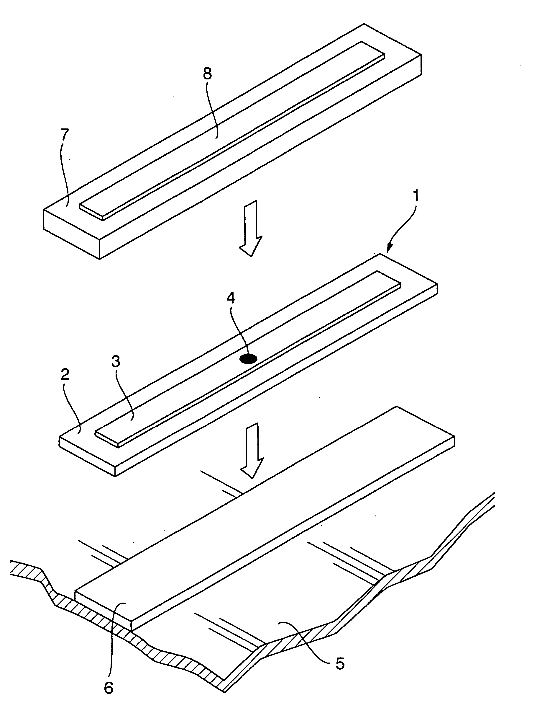
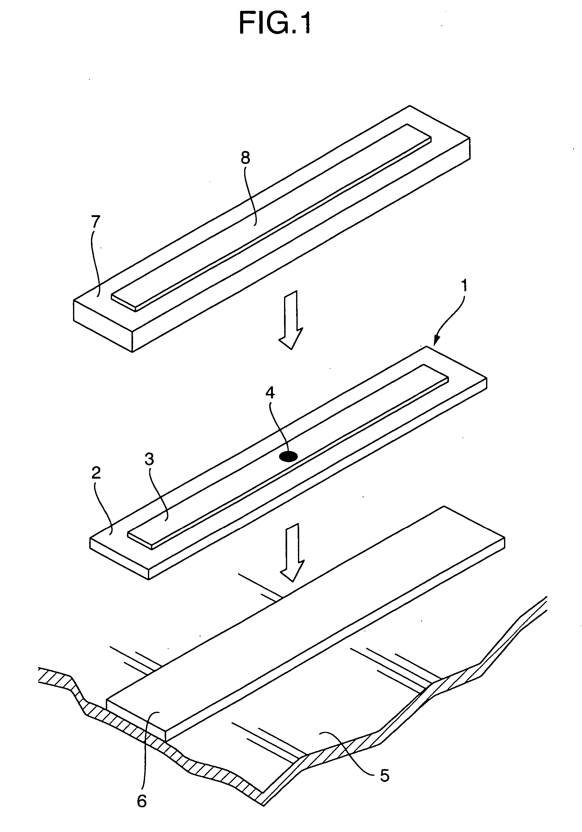
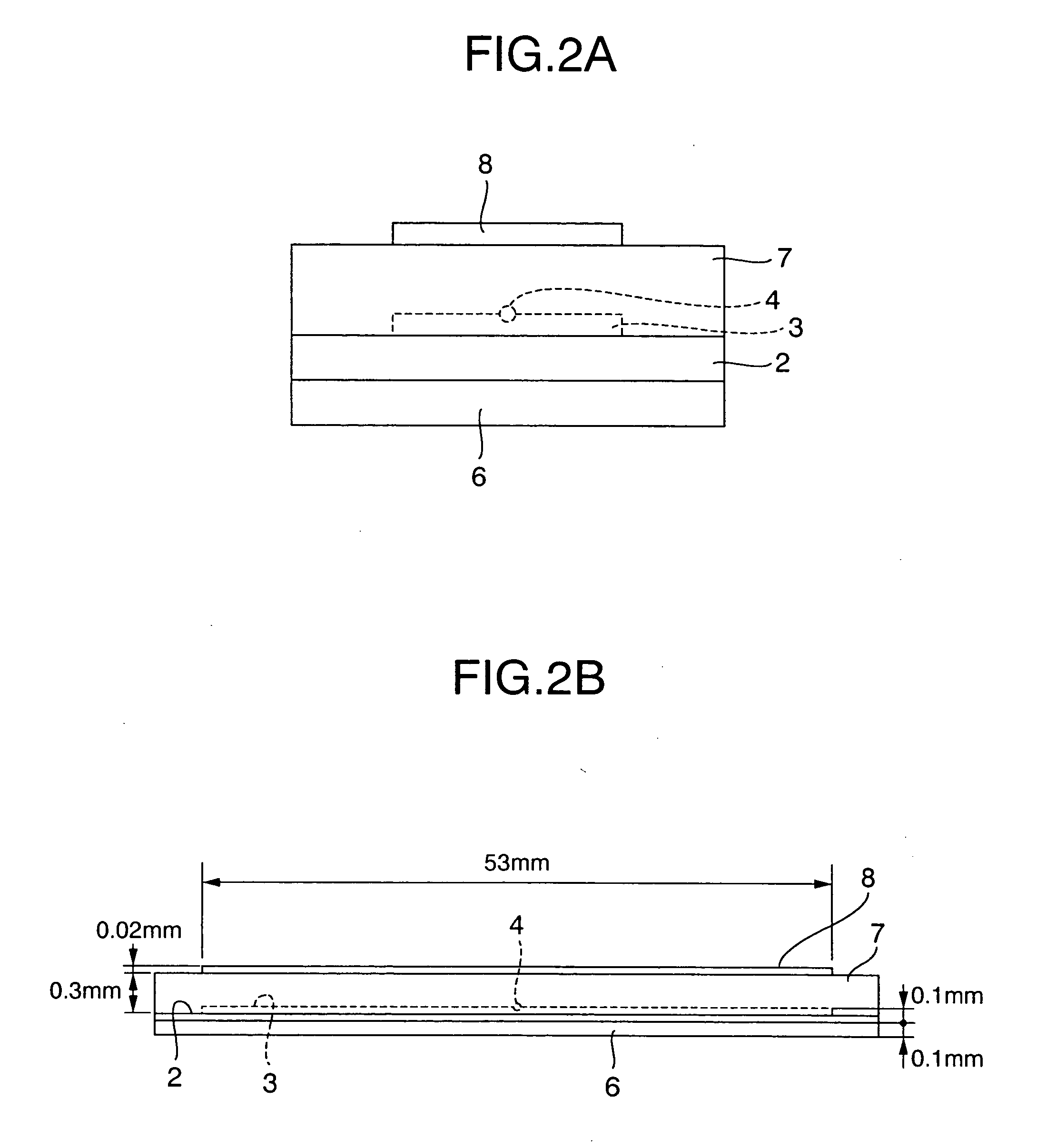
[0033]FIG. 1 shows a structure of a wireless IC tag in accordance with a first embodiment (embodiment 1). FIG. 2B is a cross-sectional view of the wireless IC tag of FIG. 1 when taken in its width direction, and FIG. 2A is a cross-sectional view of the wireless IC tag of FIG. 1 when taken in its length direction. Among members of the wireless IC tag shown in FIG. 1; a base material 2, an antenna (first antenna) 3, and an IC chip 4 form a plate shape, and are collectively called “inlet 1”. Reference numeral 5 denotes a member on which the wireless IC tag is mounted. The wireless IC tag according to embodiment 1 includes the inlet 1 having the first antenna 3 mounted on the base material 2 to be connected to the IC chip 4 having ID information stored therein, a first spacer 6 mounted on a lower surface of the inlet 1 (e.g., on the side of the inlet opposed to the metallic member 5), a second spacer 7‘mounted on an upper side of the inlet 1 (on the side of the inlet opposed to the meta...

embodiment 2

[0052]FIG. 5 schematically shows a structure of an apparatus for manufacturing such a wireless IC tag (as having the structure shown in FIG. 1). Constituent elements having the same functions or structures as in FIG. 1 are denoted by the same reference numerals. In FIG. 5, diagrams shown as surrounded by respective circles in the vicinity of an inlet material 11, a first spacer material 12, a second spacer material 13 and a second antenna material 14, to be explained later, are views of the respective materials when viewed from their planes. A diagram shown as surrounded by a circle in the lower right side of FIG. 5 is a perspective view of the wireless IC tag (having a structure similar to that of FIG. 1) manufactured by the wireless IC tag manufacturing apparatus.

[0053] In FIG. 5, reference numeral 11 denotes the first antenna material (more specifically, the inlet material). As already explained earlier, it is already known that, for example, 10,000 of the first antennas 3 conne...

embodiment 3

[0067] Explanation will next be made in connection with an embodiment when a wireless IC tag is mounted to various types of cables including a communication cable and a power cable, by comparing it with a prior art. FIGS. 10A and 10B show a conceptual view of a condition when a wireless IC tag is mounted onto a cable in the prior art, wherein FIG. 10A is a condition when the tag is mounted to a multicore cable, and FIG. 10B is a condition when the tag is mounted onto a single core cable. As shown in FIG. 10A, in a multicore cable 70 used as a communication cable, a plurality of internal conductors 72 as multiple cores each coated with single core envelope 71 are surrounded by a shield layer 73, which in turn is further covered with a cable enclosure 74. A wireless IC tag 75 is bonded onto the surface of the cable enclosure 74 with an adhesive or the like.

[0068] As shown in FIG. 10B, in a single core, cable 80 is used as a power cable, an internal conductor 81 is covered with a sing...


PUM

PropertyMeasurementUnit
thicknessaaaaaaaaaa
thicknessaaaaaaaaaa
thicknessaaaaaaaaaa

Abstract

In a wireless IC tag, metallic antennas are deposited as thin films on the front and back surfaces of a spacer, made of a heat-resistant glass epoxy material having a desired dielectric constant, to form a first antenna and a second antenna. An IC chip is mounted in the center of the first antenna. The second antenna functions as an auxiliary antenna for resonating to a desired frequency of a transmission radio wave of the first antenna to strengthen the intensity of the radio wave. Accordingly, even when the IC tag is mounted to a cable or the like, the tag can be mounted in the interior of the enclosure of the cable and thus the radio wave intensity of the first antenna can be prevented from being weakened by a metallic member in the cable.

Description

INCORPORATION BY REFERENCE [0001] The present application claims priority from Japanese applications JP 2004-221926 filed on Jul. 29, 2004, JP 2003-431025 filed on Dec. 25, 2003, the contents of which are hereby incorporated by reference into this application. BACKGROUND OF THE INVENTION [0002] The present invention relates to wireless IC tags suitable for mounting on a member having a large dielectric constant, and methods and apparatuses for manufacturing the wireless IC tags. In particular, the present invention relates to a wireless IC tag suitable for mounting on a power cable, a communication cable or the like, and a method and apparatus for manufacturing the wireless IC tag. [0003] For the purpose of article management, theft or fraud prevention; a wireless tag for obtaining information on an article in a non-contact manner has been developed and put to practical use. For example, JP-A-11-339142 discloses a tag which has a resonance circuit including a conductor functioning a...

Claims


Application Information

Patent Timeline
Patent Type & Authority Applications(United States)
IPC IPC(8): G06K7/10G06K19/00G06K19/077G08B13/22G08B13/24H01B7/36H01B13/34H01P11/00H01Q1/22H01Q1/38H01Q5/00H01Q5/55H01Q9/16H01Q19/24H01Q19/30
CPCG06K7/10178G06K19/07749G06K19/07756G06K19/07767G06K19/07771G08B13/2414H01Q19/24G08B13/2437G08B13/2445H01B17/34H01Q1/2225H01Q1/38H01Q9/16G08B13/2417G06K19/00
Inventor SAKAMA, ISAOASHIZAWA, MINORU
Owner HITACHI LTD
Why Eureka
Try Eureka