Method for manufacturing NAND type nonvolatile ferroelectric memory cell

a nonvolatile ferroelectric memory and nonvolatile technology, applied in the field of semiconductor devices, can solve the problems of short lifetime, short life, and deterioration of device operation characteristics, and achieve the effects of reducing layout area, improving operation characteristics, and high density device integration

Inactive Publication Date: 2005-06-30
HYUNDAI ELECTRONICS IND CO LTD
View PDF7 Cites 8 Cited by
  • Summary
  • Abstract
  • Description
  • Claims
  • Application Information

AI Technical Summary

Benefits of technology

[0023] An object of the present invention is to provide an NAND type non-volatile ferroelectric memory cell and a non-volatile ferroelectric memory of the same, in which numbers of access to a main cell and a reference cell are made the same, to maintain bitline induced voltages by the reference cell and by the main cell constant, for improving operation characteristics, minimizing a layout area, and permits a high density device integration.

Problems solved by technology

The frequent use of one reference cell required for reading main cells a few hundred times more than the main cells under a state the ferroelectric properties are not assured perfectly, that requires the reference cell much more operation than the main cells, causes a rapid degradation of the reference cell, resulting in a voltage instability, device operation characteristics deterioration, and short lifetime.

Method used


Image

  • Method for manufacturing NAND type nonvolatile ferroelectric memory cell
  • Method for manufacturing NAND type nonvolatile ferroelectric memory cell
  • Method for manufacturing NAND type nonvolatile ferroelectric memory cell

Examples


Embodiment Construction

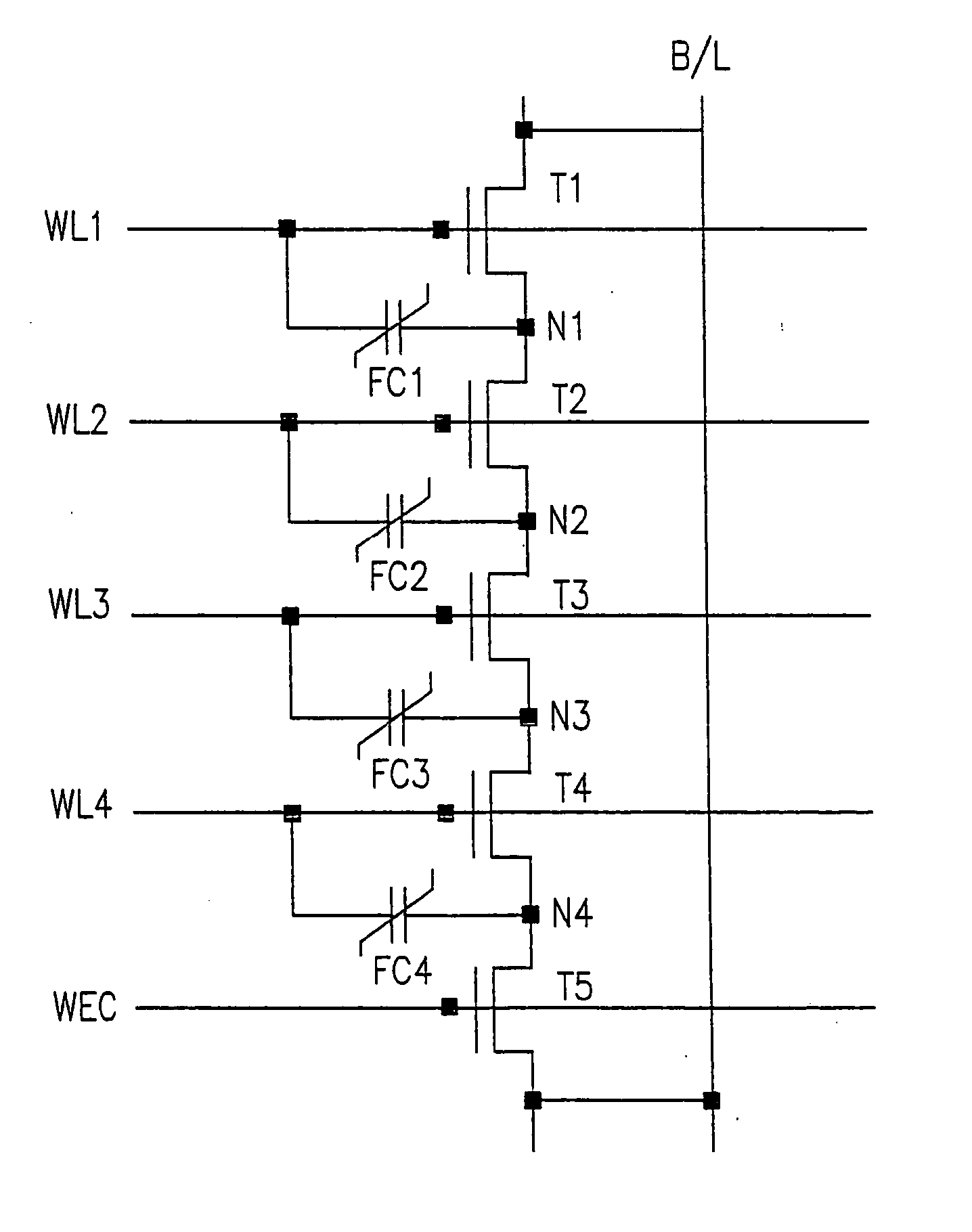
[0060] Reference will now be made in detail to the preferred embodiments of the present invention, examples of which are illustrated in the accompanying drawings. FIG. 7A illustrates a unit cell of an NAND type nonvolatile ferroelectric memory cell in accordance with a preferred embodiment of the present invention.

[0061] Referring to FIG. 7A, the unit cell is provided with NMOS transistors T1, T2, - - - T5 connected in series, and a bitline B / L formed in a direction the transistors are formed. A source of the first transistor T1 and a drain of the last transistor T5 are connected to the bitline B / L. A gate of each transistor is connected to a wordline, and a gate of the last transistor T5 is connected to a WEC signal line. The WEC signal is held disabled in a read mode and enabled only in a write mode. Ferroelectric capacitors FC1, FC2, FC3, FC4 are connected to the wordlines which are connected to gates of the transistors and drains of the transistors, but the last transistor T5 h...


PUM


Abstract

NAND type non-volatile ferroelectric memory cell and non-volatile ferroelectric memory of the same, in which numbers of access to a main cell and a reference cell are made the same, to maintain bitline induced voltages by the reference cell and by the main cell constant, for improving operation characteristics, minimizing a layout area, and permits a high density device integration, the memory cell including an N number of transistors connected in series, a bitline having an input terminal of a first transistor and an output terminal of (N)th transistor among the N number of transistors connected thereto, wordlines respectively connected to gates of the transistors except the (N)th transistor, a WEC signal line connected to a gate of the (N)th transistor and adapted to have an enable signal applied thereto only in a write or re-store mode, and ferroelectric capacitors respectively connected both to the wordlines and output terminals of the transistors.

Description

[0001] This application is a Divisional of application Ser. No. 10 / 747,944 filed on Dec. 31, 2003 which is a Divisional of application Ser. No. 10 / 223,601 filed Aug. 20, 2002 which is a Divisional of application Ser. No. 09 / 433,358 filed Nov. 4, 1999 and claims priority to Korean Patent Application No. 49741 / 1998 filed Nov. 19, 1998. The entire disclosure of the prior applications are considered as being part of the disclosure of the accompanying application and are hereby incorporated by reference therein.BACKGROUND OF THE INVENTION [0002] 1. Field of the Invention [0003] The present invention relates to a semiconductor memory, and more particularly, to an NAND type non-volatile ferroelectric memory cell and a non-volatile ferroelectric memory of the same. [0004] 2. Background of the Related Art [0005]FIG. 1 illustrates a system of a related art NAND type DRAM. [0006] Referring to FIG. 1, the NAND type DRAM cell is provided with a plurality of NMOS transistors T1, T2, T3, - - - con...

Claims


Application Information

Patent Timeline
Patent Type & Authority Applications(United States)
IPC IPC(8): G11C11/22G11C14/00H01L21/8246H01L21/8247H01L27/10H01L27/115H01L29/788H01L29/792
CPCG11C11/22H01L27/11507H01L27/11502H10B53/30H10B53/00
Inventor KANG, HEE BOK
Owner HYUNDAI ELECTRONICS IND CO LTD
Why Eureka
Try Eureka