Check patentability & draft patents in minutes with Patsnap Eureka AI!

Semiconductor memory device with optimum refresh cycle according to temperature variation

a memory device and temperature variation technology, applied in the field of semiconductor memory devices, can solve the problems of consuming a lot of power, reducing the charge quantity of the capacitor, and reducing the efficiency of the semiconductor memory device,

Inactive Publication Date: 2005-06-30
SK HYNIX INC
View PDF7 Cites 45 Cited by
  • Summary
  • Abstract
  • Description
  • Claims
  • Application Information

AI Technical Summary

Benefits of technology

[0030] It is, therefore, an object of the present invention to provide a semiconductor memory device having an optimum refresh cycle for performing a refresh operation consuming low power.

Problems solved by technology

However, charge quantity stored in the capacitor reduces as time passes.
Therefore, if the refresh cycle is set to be suitable for only a room temperature, data stored in the semiconductor memory device may be easily lost when temperature is higher than the room temperature.
However, since the refresh cycle is fixed for the highest operational temperature, the semiconductor memory device performs a refresh operation too frequently consuming much power even if temperature is much lower than the highest operational temperature.
However, the conventional semiconductor memory device can have only two different periods of the refresh signal.
Therefore, the conventional semiconductor memory device cannot control the period of the refresh signal precisely.
In addition, when the conventional semiconductor memory device is operated, a temperature variation of the conventional semiconductor memory device is usually small.
In this case, a circuit included in the conventional semiconductor memory device for controlling the period of the refresh signal may be useless.

Method used


Image

  • Semiconductor memory device with optimum refresh cycle according to temperature variation
  • Semiconductor memory device with optimum refresh cycle according to temperature variation
  • Semiconductor memory device with optimum refresh cycle according to temperature variation

Examples


first embodiment

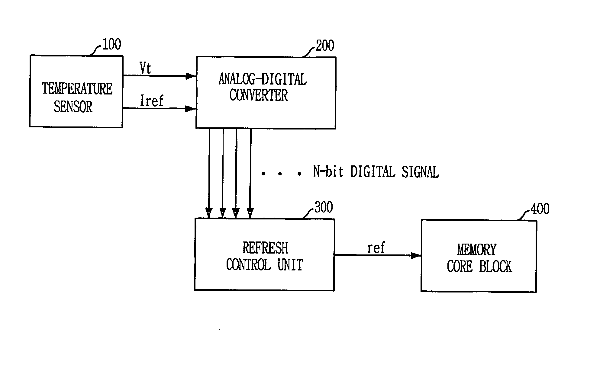
[0047]FIG. 5 is a block diagram showing a semiconductor memory device in accordance with the present invention.

[0048] As shown, the semiconductor memory device includes a temperature sensor 100, an analog-digital converter 200, a refresh controller 300 and a memory core block 400.

[0049] The temperature sensor 100 measures temperature of the semiconductor memory device in order to output a temperature controlled voltage signal Vt and a reference current Iref according to the measured temperature. Herein, the temperature sensor 100 is turned on while the semiconductor memory device is turned on in order to accurately measure the temperature of the semiconductor memory device.

[0050] The analog-digital converter 200 generates an N-bit digital signal in response to the temperature controlled voltage signal Vt for controlling the refresh controller 300.

[0051] The refresh controller 300 generates a refresh signal ref in response to the N-bit digital signal. The memory core block 400 per...

second embodiment

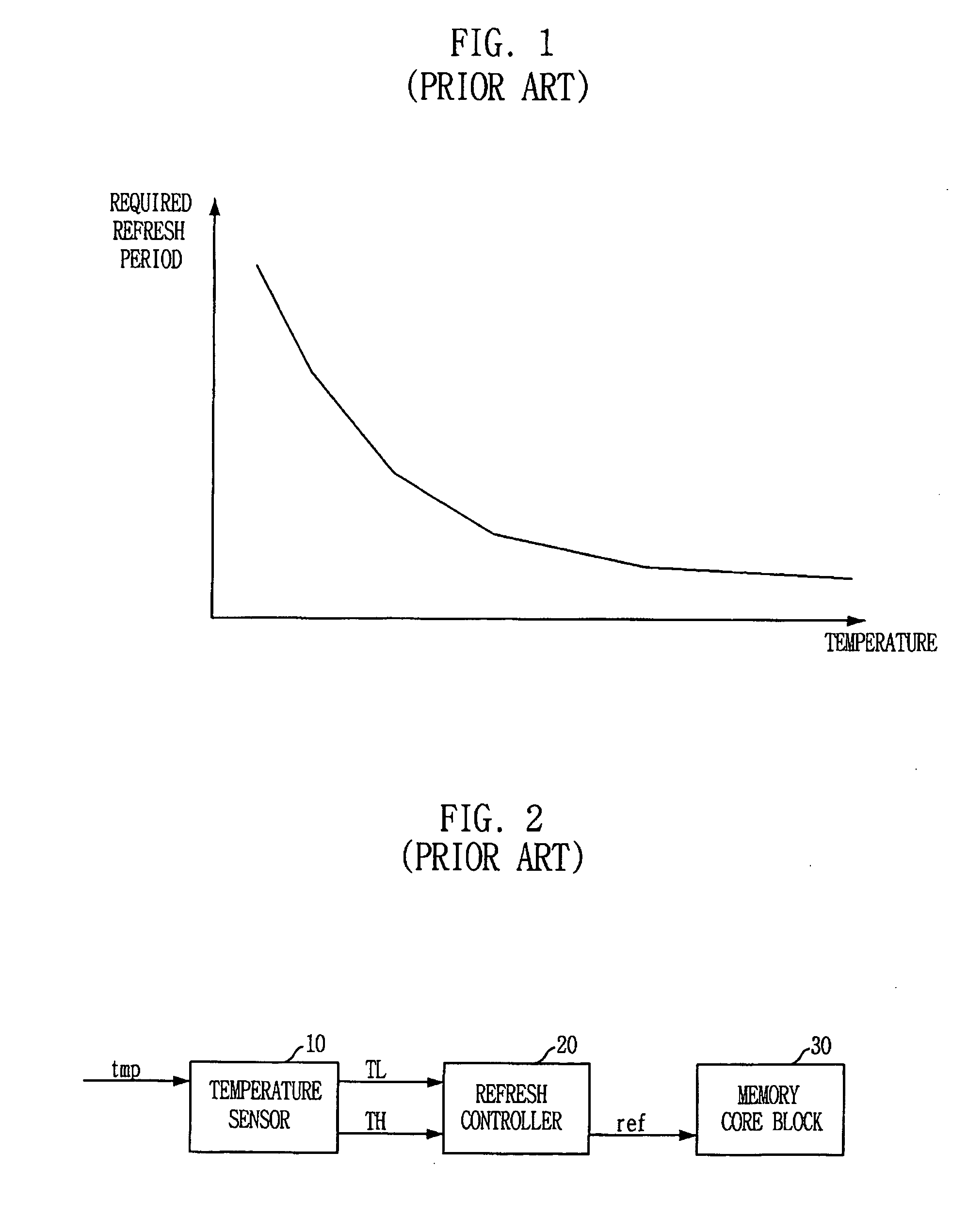
[0134]FIG. 11 is a schematic circuit diagram showing a semiconductor memory device in accordance with the present invention.

[0135] As shown, the semiconductor memory device includes a temperature sensor 100, a voltage controlled oscillator and a memory core block 400.

[0136] The temperature sensor 100 measures temperature of the semiconductor memory device in order to generate a temperature controlled voltage signal Vt according to the measured temperature.

[0137] The refresh controller 300 generates a refresh signal ref based on the temperature controlled voltage signal Vt.

[0138] The memory core block 400 performs a refresh operation in response to the refresh signal ref.

[0139] Structures and operations of the temperature sensor 100 and the memory core block 400 are the same as those of the temperature sensor 100 and the memory core block 400 shown in FIG. 5. Therefore, detailed descriptions of the temperature sensor 100 and the memory core block 400 are omitted.

[0140] The volta...


PUM


Abstract

A semiconductor memory device, which performs a refresh operation, includes: a temperature sensing unit for measuring temperature and for generating a temperature controlled voltage and a reference current based on the measured temperature; an analog-digital conversion unit for converting the temperature controlled voltage to an N-bit digital signal; a refresh control unit for generating a refresh signal in response to the N-bit digital signal, wherein, a period of the refresh signal is controlled based on the N-bit digital signal.

Description

FIELD OF INVENTION [0001] The present invention relates to a semiconductor memory device; and, more particularly, to a semiconductor memory device capable of controlling a refresh cycle according to a temperature variation. DESCRIPTION OF PRIOR ART [0002] Generally, a semiconductor memory device is classified into two different types: one is a dynamic random access memory (DRAM) and the other is a static random access memory (SRAM). [0003] Since a memory cell included in the SRAM is formed by four latched transistors, the SRAM can hold its data without a refresh operation as long as power is supplied to the SRAM. [0004] In contrast, a memory cell included in the DRAM is formed by a transistor and a capacitor; and the capacitor is charged or discharged for the DRAM operation. However, charge quantity stored in the capacitor reduces as time passes. Therefore, the DRAM must be refreshed periodically in order to hold its data contents. [0005] A refresh cycle is required to be changed ac...

Claims


Application Information

Patent Timeline
Patent Type & Authority Applications(United States)
IPC IPC(8): G11C11/401G11C7/00G11C11/406
CPCG11C11/406G11C2211/4061G11C11/40626G11C11/401
Inventor KIM, SE-JUNHONG, SANG-HOONKO, JAE-BUM
Owner SK HYNIX INC
Features
  • R&D
  • Intellectual Property
  • Life Sciences
  • Materials
  • Tech Scout
  • Unparalleled Data Quality
  • Higher Quality Content
  • 60% Fewer Hallucinations
Learn More