Low latency optical memory bus

a memory bus and low-latency technology, applied in the field of memory bus, can solve the problems of impedance discontinuity, electrical noise and time delay, and limitations of the memory bus architectur

Inactive Publication Date: 2005-07-07
INTEL CORP
View PDF13 Cites 40 Cited by
  • Summary
  • Abstract
  • Description
  • Claims
  • Application Information

AI Technical Summary

Problems solved by technology

This memory bus architecture has limitations, however.
For example, plugging multiple memory modules into the bus causes impedance discontinuities.
Impedance discontinuities can cause electrical noise and time delays due to signal reflections.
Buffering adds latency, however, which is a performance limiter as well.

Method used


Image

  • Low latency optical memory bus
  • Low latency optical memory bus
  • Low latency optical memory bus

Examples


Embodiment Construction

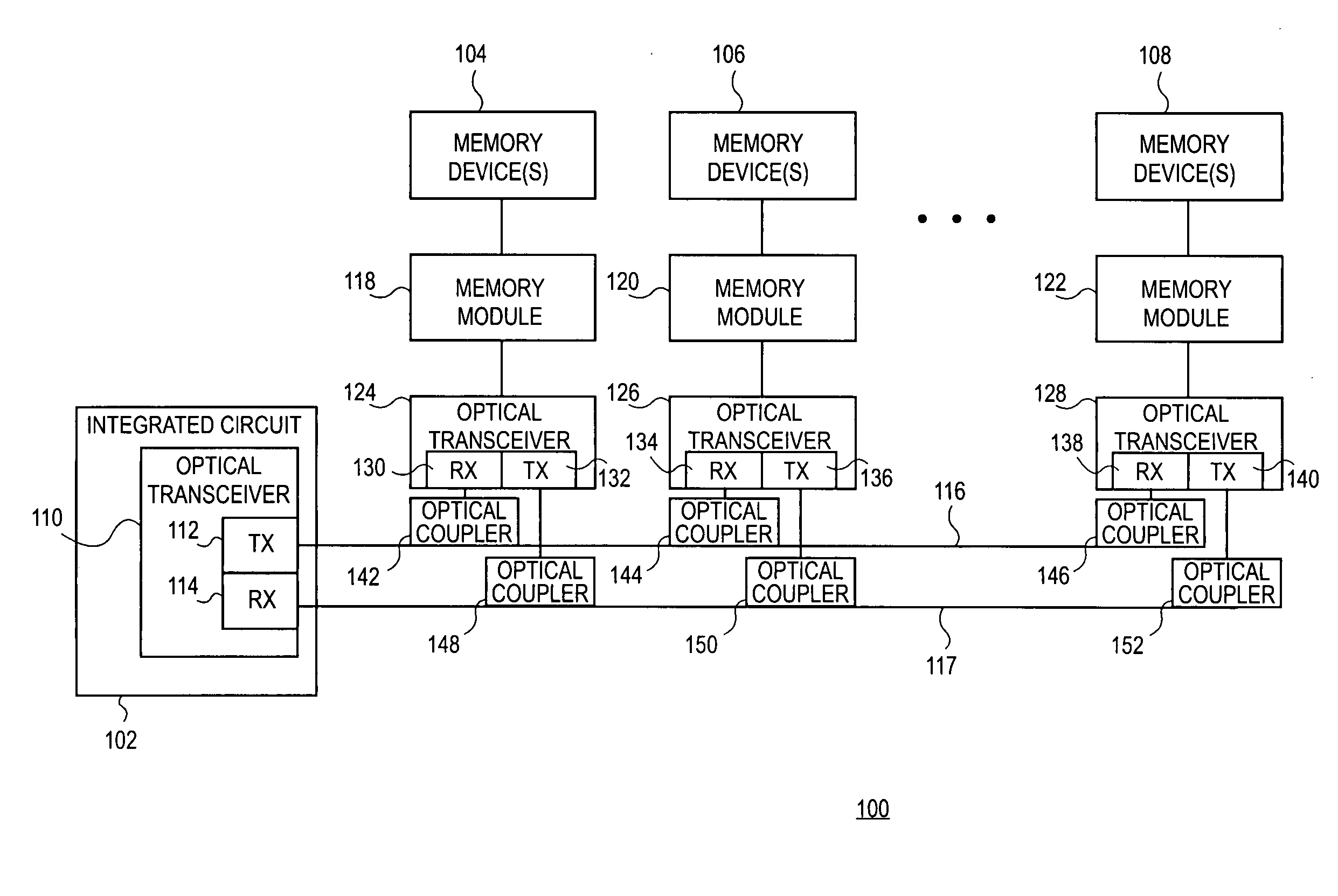
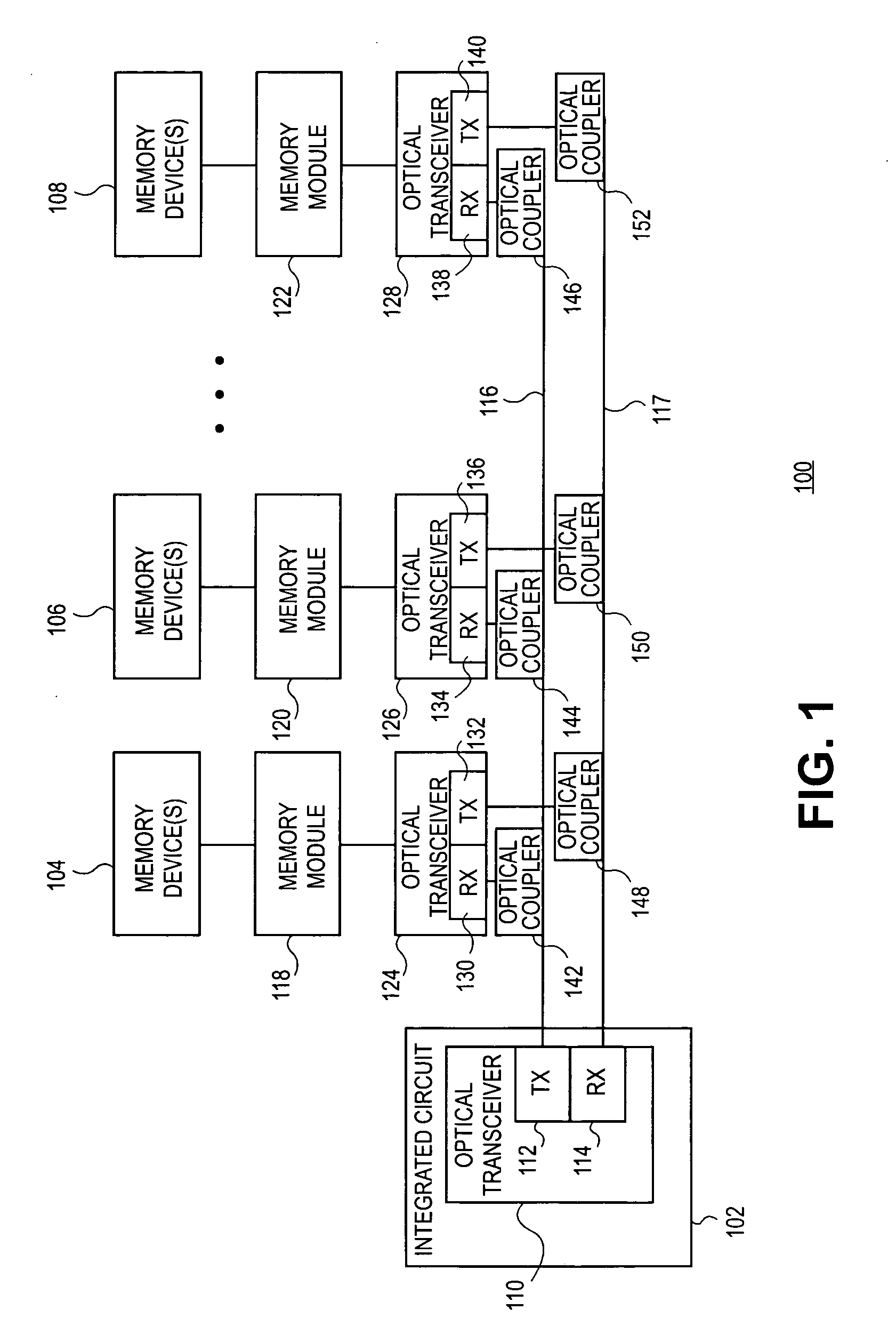
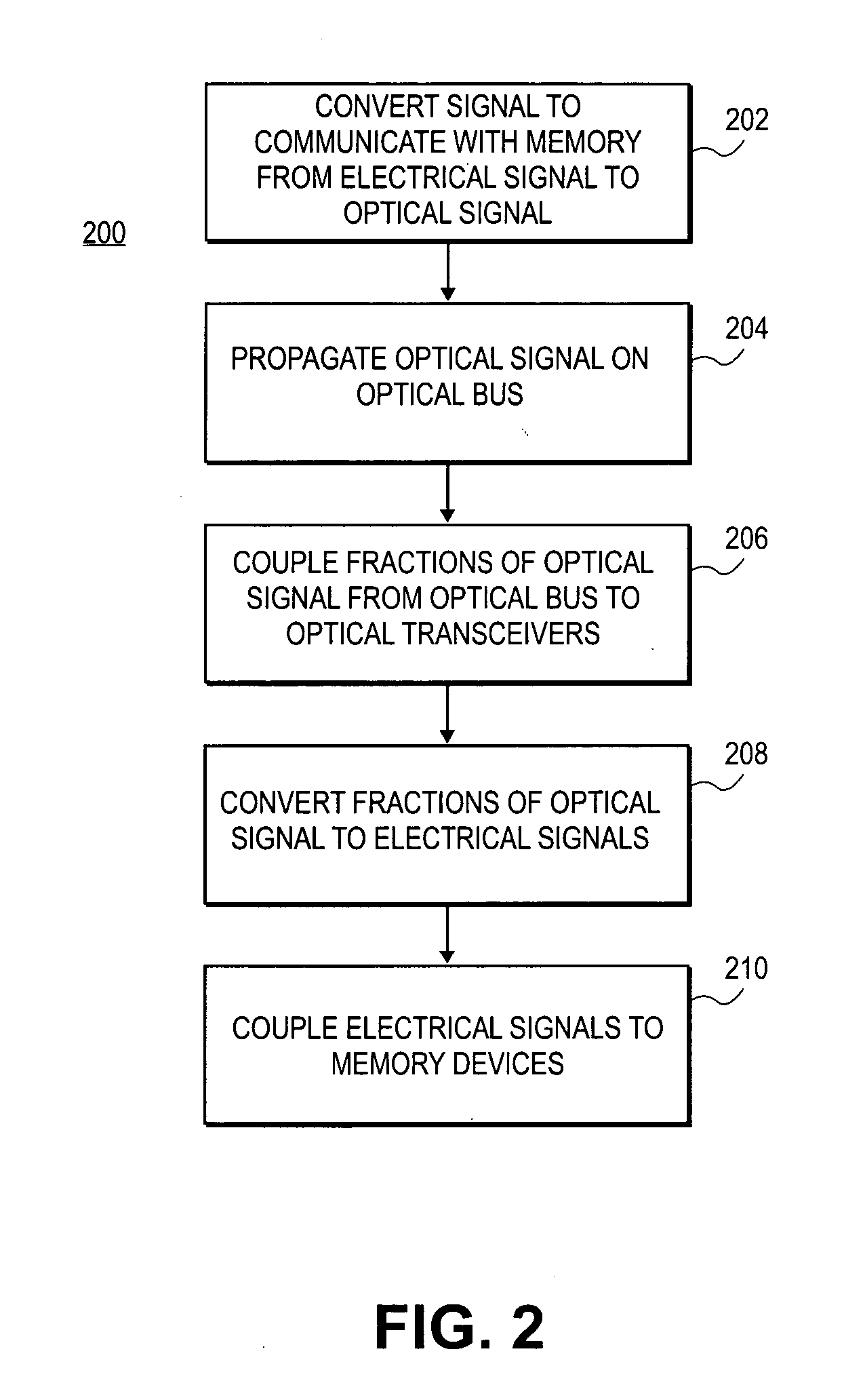
[0013]FIG. 1 is a high level schematic diagram of a memory subsystem 100 according to an embodiment of the present invention. The memory subsystem 100 includes an integrated circuit 102 to communicate with one or more memory devices, such as the memory devices 104, 106, and 108. In the illustrated embodiment, the integrated circuit 102 includes an optical transceiver 110, which includes an optical transmitter 112 and an optical receiver 114. The optical transmitter 112 is coupled to an optical bus 116 and the optical receiver 114 is coupled to an optical bus 117.

[0014] In the illustrated embodiment, the memory devices 104, 106, and 108 are coupled to memory modules 118, 120, and 122, respectively. The memory modules 118, 120, and 122 are coupled to optical transceivers 124, 126, and 128, respectively. The optical transceiver 124 includes an optical receiver 130 and an optical transmitter 132. The optical transceiver 126 includes an optical receiver 134 and an optical transmitter 13...


PUM


Abstract

Embodiments of the present invention include an integrated circuit to communicate with a memory device. The integrated circuit includes an optical transmitter and an optical bus coupled to the integrated circuit's optical transmitter. N optical receivers are coupled to the optical bus via N optical couplers. N memory modules are coupled to the N optical receivers. M memory devices are coupled to the N memory modules. The optical transmitter converts a signal to communicate with the N memory modules from an electrical signal to an optical signal. The optical bus propagates the optical signal. Each of the N optical couplers to couple a one-Nth of the optical signal from the optical bus to each one of the N optical receivers, each of the N optical receivers converts its one-Nth of the optical signal to an electrical signal for its associated memory device.

Description

BACKGROUND [0001] 1. Field [0002] Embodiments of the present invention relate to memory circuits and particularly to memory buses. [0003] 2. Discussion of Related Art [0004] A common computer chipset includes a processor electrically coupled to a memory controller via a front side bus. The memory controller is electrically coupled to one or more memory modules via a memory bus. The memory modules plug into the memory bus and memory devices plug into the memory modules. The processor can read from the memory devices and / or write to the memory devices. For efficient operation of the chipset, the processor should have high-speed access to the memory devices. As technology advances, it is common to increase the speed of the memory bus to improve the performance of the chipset. [0005] One memory bus architecture that supports faster bus speeds uses multiple memory modules. In this architecture, several memory modules can be plugged into the memory bus for each memory channel that the mem...

Claims


Application Information

Patent Timeline
Patent Type & Authority Applications(United States)
IPC IPC(8): G02B6/43G06F13/16
CPCG06F13/1668G02B6/28G02B6/43H04B10/25
Inventor MORROW, WARREN R.BARNETT, BRANDON C.
Owner INTEL CORP
Why Eureka
Try Eureka