Semiconductor device and method for testing the same

a technology of semiconductors and devices, applied in the direction of measurement devices, electronic circuit testing, instruments, etc., can solve the problems of the circuit area, and achieve the effect of increasing the circuit area and increasing the die size of the lsi

Inactive Publication Date: 2005-07-07
FUJITSU LTD
View PDF14 Cites 6 Cited by
  • Summary
  • Abstract
  • Description
  • Claims
  • Application Information

AI Technical Summary

Benefits of technology

[0013] However, such conventional memory-embedded LSI provided with a test circuit requires a circuit for decoding a test code and a plurality of test terminals for providing test signals. This increases the circuit area, which leads to a problem that the die size of the LSI is increased.

Problems solved by technology

This increases the circuit area, which leads to a problem that the die size of the LSI is increased.

Method used


Image

  • Semiconductor device and method for testing the same
  • Semiconductor device and method for testing the same
  • Semiconductor device and method for testing the same

Examples


Embodiment Construction

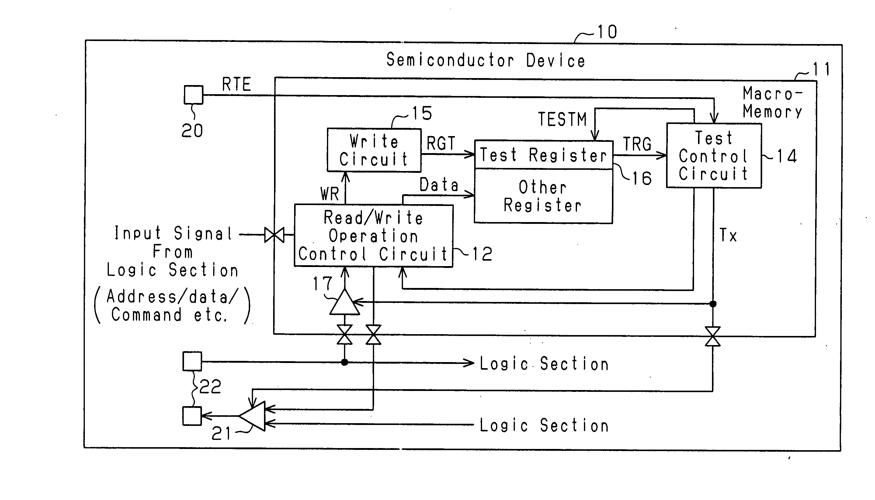
[0031]FIG. 1 is a schematic block diagram showing a semiconductor device 10 according to an embodiment of the present invention. The semiconductor device 10 includes a memory section (macro memory) 11 that is mounted together with a logic section. The macro memory 11 is provided with an operation control circuit 12 for performing a data read / write operation based on an input signal containing an address, data, and a command. A test memory circuit 16 for storing data to select a test mode is provided in a storage area (address space) selected by the address contained in the input signal. A write circuit 15 provides a control signal RGT, which enables writing of data to the test memory circuit 16, in response to a write command WR provided from the operation control circuit 12. The data Data contained in the input signal is written to the test memory circuit 16 based on the control signal RGT.

[0032] The operation control circuit 12 is a circuit for accessing register area and memory ...


PUM


Abstract

A semiconductor device capable that shortens test time with a simple circuit configuration and prevents enlargement of the circuit area for testing. The semiconductor device has a macro memory and a logic section mounted thereon. The macro memory includes an operation control circuit for executing a read/write operation of data in accordance with an input signal containing an address, data, and a command. A test register for storing data to select a test mode is arranged in a storage area of the macro memory that is selected by an address. A write circuit generates a control signal enabling the writing of data to the test register in response to a write command provided from the operation control circuit.

Description

CROSS-REFERENCE TO RELATED APPLICATIONS [0001] This application is a continuation of, and claims priority from International PCT Application No. PCT / JP03 / 016156, filed on Dec. 17, 2003, the contents being incorporated herein in entirety by reference.BACKGROUND OF THE INVENTION [0002] The present invention relates to a semiconductor device having a logic section and a memory section mounted together on a single chip and a test method thereof. [0003] In the recent trend of high integration of semiconductor devices (LSIs), such as ASICs and microprocessors, LSIs have become to have a macro memory (memory section) mounted together with a logic section on the same chip. Such memory-embedded LSIs are subjected to a performance test before shipping to check whether the logic sections and macro memories operate normally. There is a demand for technology that shortens the test time for macro memories with a simple circuit configuration. [0004] In a memory-embedded LSI, ordinary operations (w...

Claims


Application Information

Patent Timeline
Patent Type & Authority Applications(United States)
IPC IPC(8): G01R31/28G01R31/317G11C29/16
CPCG01R31/31701G11C29/16G01R31/31723
Inventor FURUYAMA, TAKAAKI
Owner FUJITSU LTD
Why Eureka
Try Eureka