Semiconductor light emitting device and plant cultivating system

a technology of light emitting device and semiconductor, which is applied in the direction of electrical apparatus construction details, semiconductor lasers, and energy saving measures, etc., can solve the problems of rust, clogging of cooling water passages, and rust generated in the cooling water passage of the heat sink, so as to prevent clogging of the cooling water passage and stably irradiate

Inactive Publication Date: 2005-07-14
HAMAMATSU PHOTONICS KK
View PDF7 Cites 1 Cited by
  • Summary
  • Abstract
  • Description
  • Claims
  • Application Information

AI Technical Summary

Benefits of technology

[0007] Since the conductive member provided separately in the upstream direction or in the downstream direction of the water conveyance piping has an equal potential to the conductive portion of the cooling water passage according to the above semiconductor light emitting device, the electric current hardly flows between the conductive member and the conductive portion of the cooling water passage, and rusting in the M pieces of light emitting units is inhibited. Thereby a clogged piping of the cooling water passage is prevented.
[0008] In the plant cultivation apparatus according to the present invention, the semiconductor light emitting device irradiates plants with light to cultivate the plants. According to the plant cultivation apparatus, the light necessary for cultivating the plants can be stably irradiated for a long period of time.

Problems solved by technology

The oxygen generated rusts the cooling water passage of the heat sink.
An increase in the amount of rust causes a clogged piping in the cooling water passage.
In other words, when the electric current flows through the cooling water, a clogged piping may be generated in the cooling water passage.

Method used


Image

  • Semiconductor light emitting device and plant cultivating system
  • Semiconductor light emitting device and plant cultivating system
  • Semiconductor light emitting device and plant cultivating system

Examples


Embodiment Construction

[0017] Hereinafter, the embodiment of the present invention will be described in detail with reference to the accompanying drawings. In the description of the drawings, identical components or corresponding elements are designated by the same reference numerals, and overlapping description is omitted.

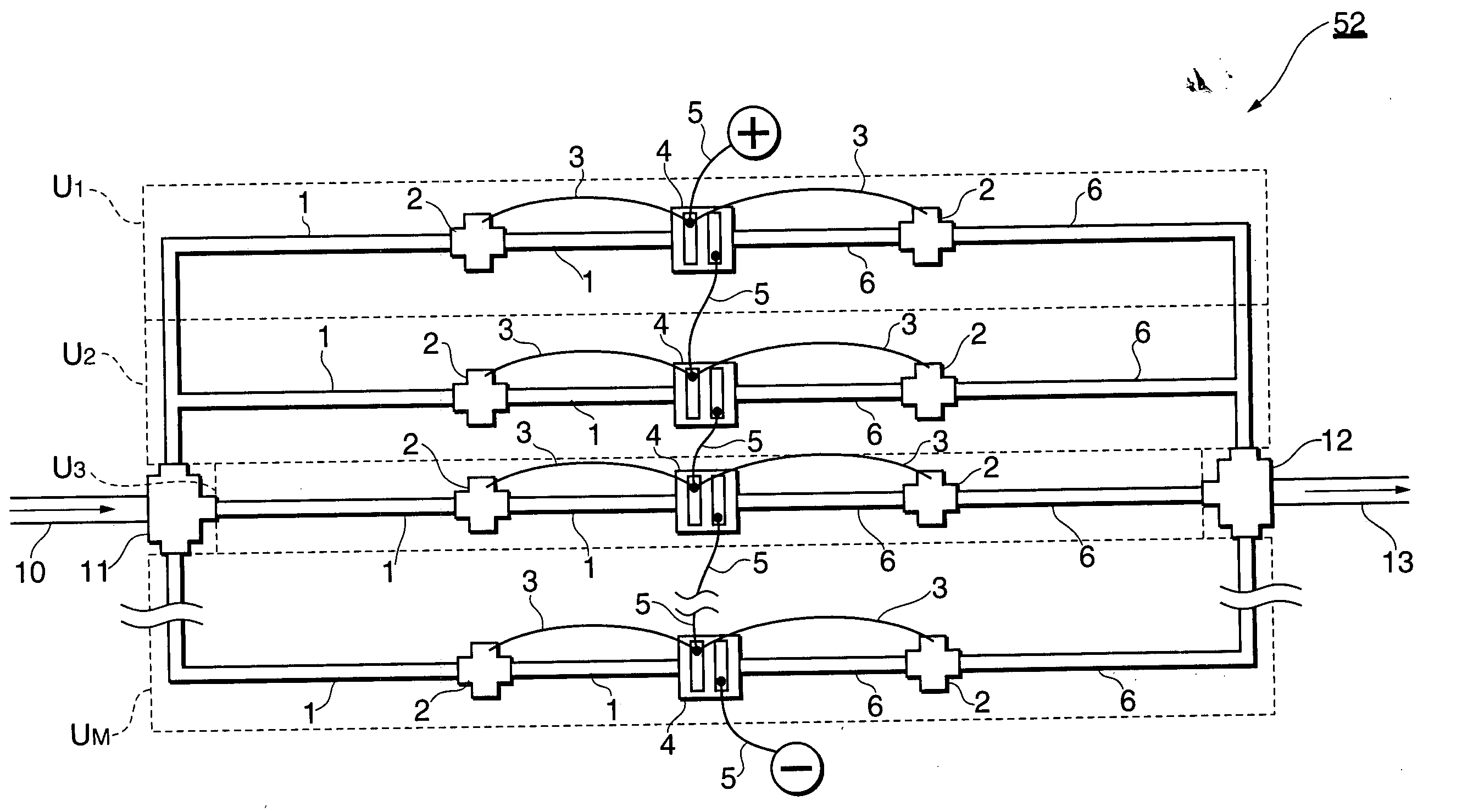
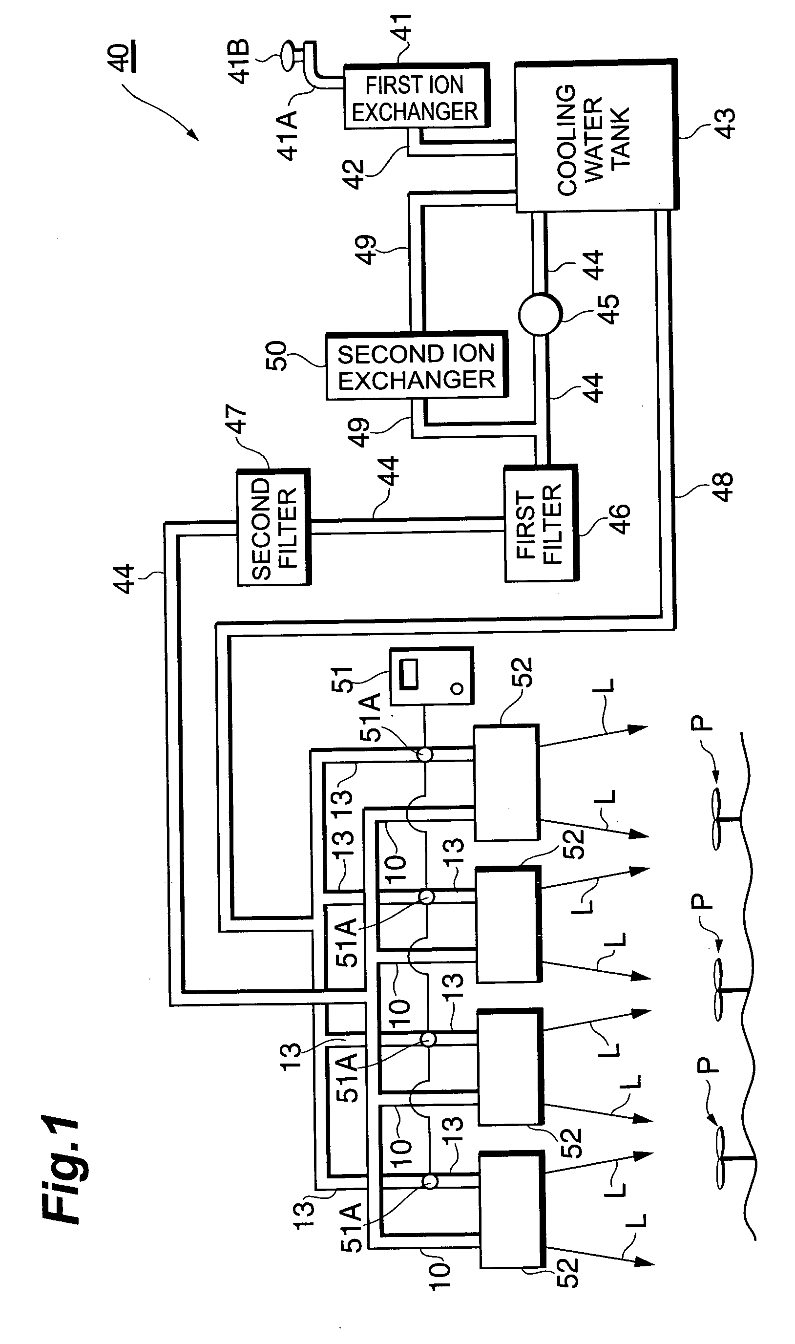
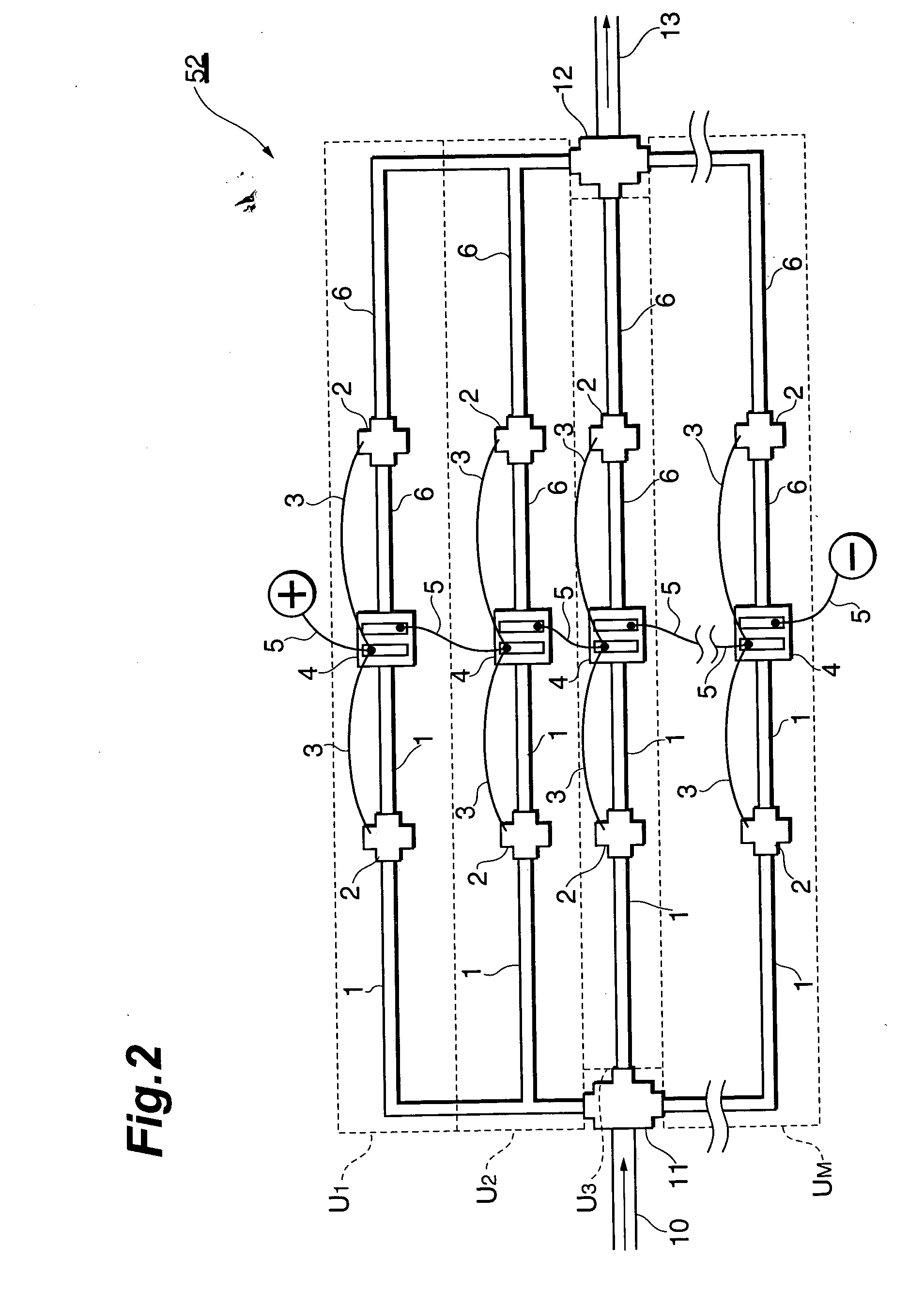
[0018]FIG. 1 is a block diagram showing an embodiment of a plant cultivation apparatus according to the present invention. The plant cultivation apparatus 40 irradiates plants P with a light L from a semiconductor light emitting element (semiconductor laser) to cultivate the plants P. As shown in FIG. 1, a first ion exchanger 41 is connected with a water pipe 41A, and chlorine ions or the like are removed from tap water supplied by operating a faucet 41B. Then, the water is supplied to a cooling water tank 43 through a cooling water supply pipe 42. For instance, the cooling water tank 43 can store cooling water of 2 t (ton) or less. A water inlet pipe 44 for the passage of the cooling ...


PUM

PropertyMeasurementUnit
conductivityaaaaaaaaaa
electric poweraaaaaaaaaa
distanceaaaaaaaaaa

Abstract

Guard electrodes 2 which are electrically connected with a conductive portion of a cooling water passage 23 through connection lines 3 are respectively provided in the middle of a water inlet pipe 1 connected with a water inlet master pipe 10 and a water outlet pipe 6 connected with a water outlet master pipe 13 in M pieces of semiconductor laser units 4. At this time, since the guard electrode 2 has a potential equal to the conductive portion of the cooling water passage 23, the electric current hardly flows between the guard electrode 2 and the conductive portion of the cooling water passage 23. As a result, rusting is inhibited in the M pieces of semiconductor laser units 4, and a clogged piping is prevented in the cooling water passage 23.

Description

FIELD OF THE ART [0001] The present invention relates to a semiconductor light emitting device using a semiconductor light emitting element such as a semiconductor laser, for example, relates to a semiconductor light emitting device used for micro fabrication process and plant cultivation or the like. BACKGROUND ART [0002] In a semiconductor laser array in which a plurality of semiconductor laser elements as one of semiconductor light emitting elements are arranged, a laser output is generally saturated due to a temperature increase. Therefore, a heat sink which cools the semiconductor laser array is used with the semiconductor laser array. For instance, these techniques are disclosed in “O plus E 1999-2 Vol. 21 No. 2(p. 173-178)” and Japanese Patent Application Laid-Open No. H8-139479. According to the techniques, the semiconductor laser array is cooled by cooling water passing through a cooling water passage provided in the heat sink, and thereby the laser output is prevented from...

Claims


Application Information

Patent Timeline
Patent Type & Authority Applications(United States)
IPC IPC(8): H01L23/473A01G7/04H01S5/024
CPCA01G7/045H01L23/473Y10T29/49158H01L2924/0002H01L2924/00A01G9/249Y02P60/14
Inventor HONMA, TAKAYOSHITSUCHIYA, HIROSHIKAN, HIROFUMI
Owner HAMAMATSU PHOTONICS KK
Why Eureka
Try Eureka