Dielectric layer for semiconductor device and method of manufacturing the same

a semiconductor device and dielectric layer technology, applied in semiconductor devices, capacitors, electrical apparatus, etc., can solve the problems of unresolved problems associated with conventional dielectric materials, unsatisfactory efforts to solve the problems of conventional dielectric materials, and the difficulty of scaling down of silicon dioxide gate dielectrics

Inactive Publication Date: 2005-07-14
SAMSUNG ELECTRONICS CO LTD
View PDF16 Cites 301 Cited by
  • Summary
  • Abstract
  • Description
  • Claims
  • Application Information

AI Technical Summary

Benefits of technology

[0012] In one embodiment, a semiconductor device comprises a silicate interface layer and a high-k dielectric layer overlying the silicate interface layer. The high-k dielectric layer comprises metal alloy oxides.

Problems solved by technology

However, because the silicon dioxide has a low dielectric constant (k), e.g., 3.9, further scaling down of silicon dioxide gate dielectric has become more and more difficult.
As a result, a gate-to-channel leakage current through thin silicon dioxide gate dielectrics increases, leading to an undesirable power consumption problem.
However, such attempts have not succeeded in solving the problems associated with the conventional dielectric materials.
For example, the silicon nitride layer or oxynitride layer between the high-k dielectric layer and the silicon substrate or the polysilicon gate electrode causes charge trapping with high interface state densities, thereby reducing channel mobility and also degrading device performance.
Further, the formation of the silicon nitride layer or the oxynitride layer requires a relatively large thermal budget.

Method used


Image

  • Dielectric layer for semiconductor device and method of manufacturing the same
  • Dielectric layer for semiconductor device and method of manufacturing the same
  • Dielectric layer for semiconductor device and method of manufacturing the same

Examples


Embodiment Construction

[0020] The present invention provides a noble dielectric layer structure and a method of manufacturing the same. In the following description, numerous specific details are set forth to provide a thorough understanding of the present invention. However, one having ordinary skill in the art should recognize that the invention can be practiced without these specific details. In some instances, well-known process steps, device structures, and techniques have not been shown in detail to avoid obscuring the present invention.

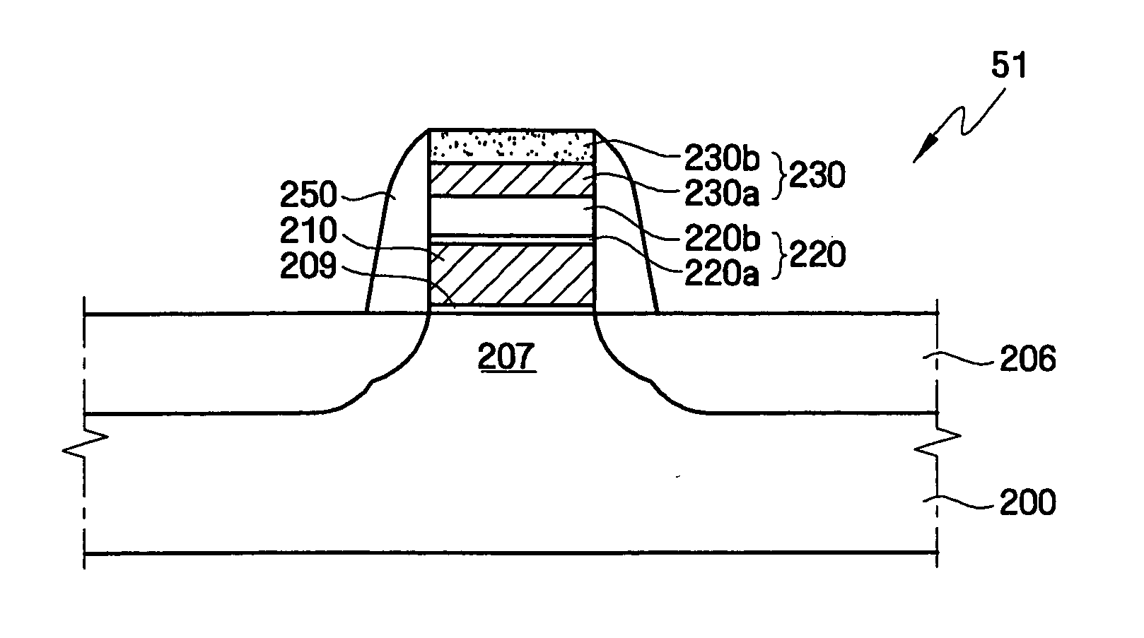
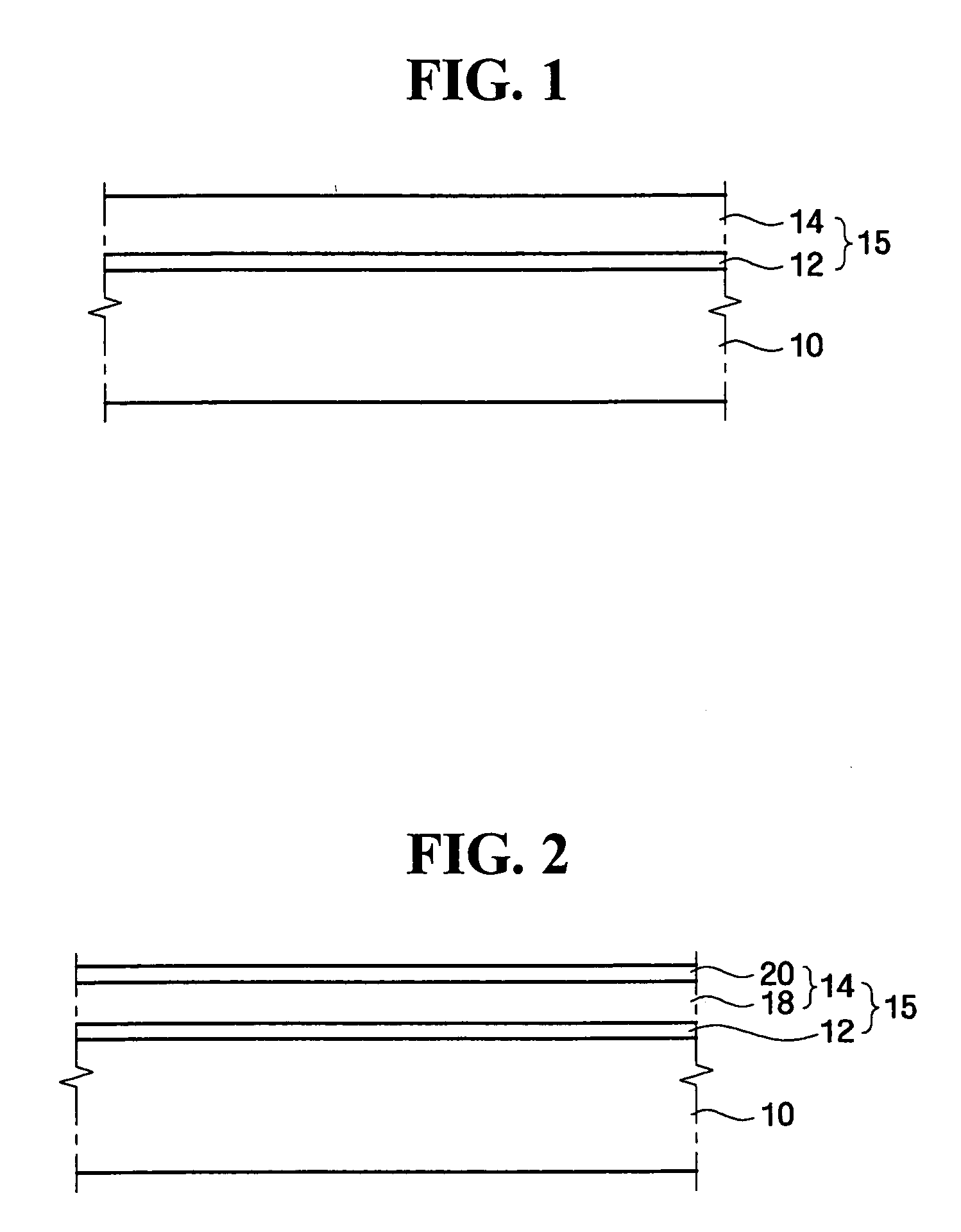
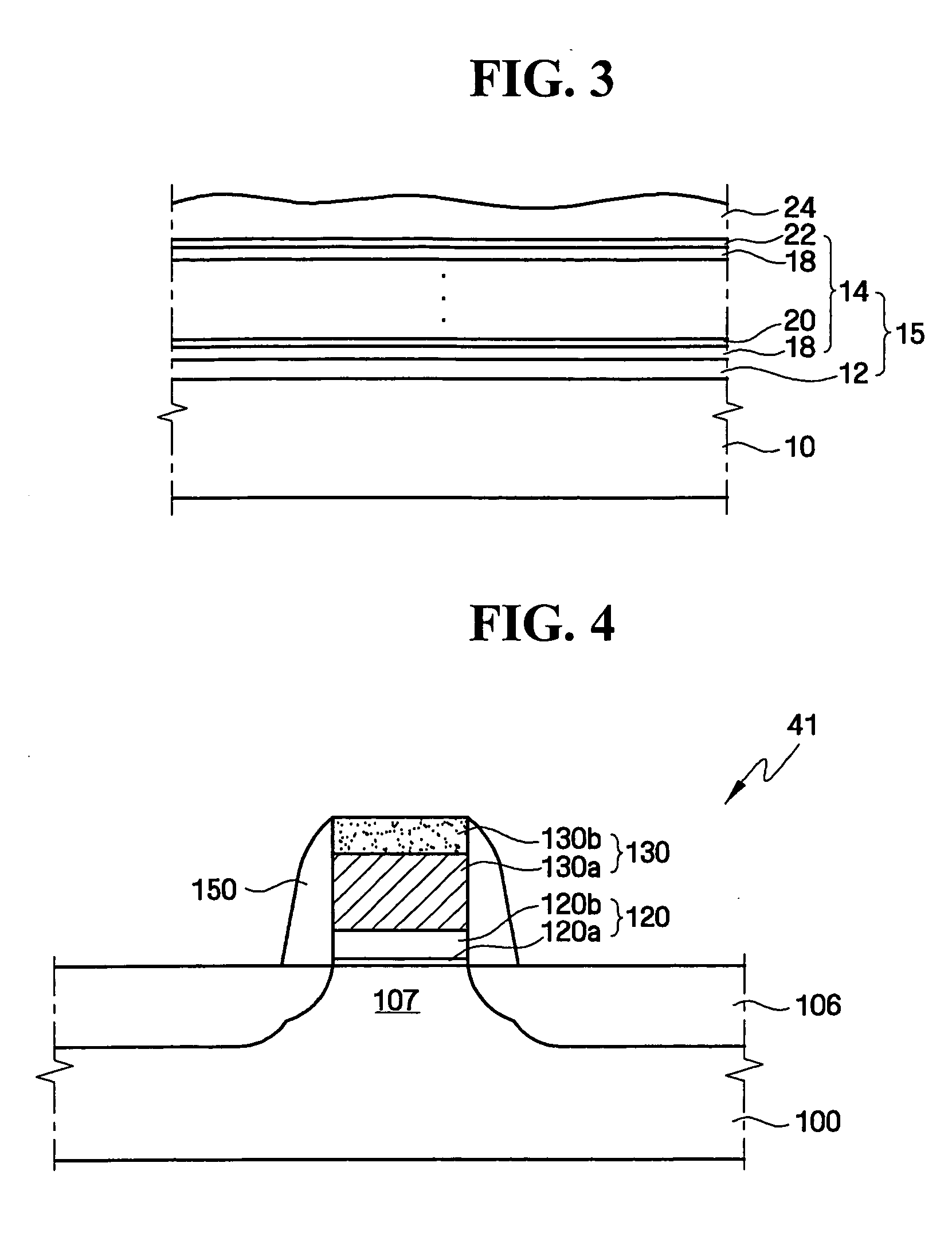
[0021] Referring to FIG. 1, according to an embodiment of the present invention, a silicate interface layer 12 formed of a silicate material may be disposed on a conductive layer or semiconductor substrate 10 such as a silicon substrate. The dielectric constant of the silicate interface layer 12 is preferably greater than any one of silicon oxide, silicon nitride or silicon oxynitride. Preferably, the silicate interface layer 12 has a thickness of approximately 5-50...


PUM

PropertyMeasurementUnit
thicknessaaaaaaaaaa
thicknessaaaaaaaaaa
thicknessaaaaaaaaaa

Abstract

A semiconductor device comprises a silicate interface layer and a high-k dielectric layer overlying the silicate interface layer. The high-k dielectric layer comprises metal alloy oxides.

Description

[0001] This application is a continuation-in-part (CIP) of U.S. patent application Ser. No. 09 / 776,059 filed on Feb. 2, 2001 and now pending, which is incorporated herein by reference in its entirety. This patent application also claims priority from Korean Patent Application No. 2004-5817, filed Jan. 29, 2004, the contents of which are hereby incorporated by reference in their entirety.BACKGROUND OF THE INVENTION [0002] 1. Field of the Invention [0003] This invention relates generally to the field of semiconductor devices, and more particularly, to a multi-layer dielectric structure and semiconductor devices employing the multi-layer dielectric structure and a method of manufacturing the same. [0004] 2. Description of the Related Art [0005] With each generation of metal oxide semiconductor (MOS) integrated circuit (IC), the device dimensions have been continuously scaled down to provide for high-density and high-performance devices. Particularly, the thickness of gate dielectrics i...

Claims


Application Information

Patent Timeline
Patent Type & Authority Applications(United States)
IPC IPC(8): H01L21/28H01L29/51H01L29/788H01L29/94
CPCH01L21/28185H01L21/28194H01L21/28202H01L28/56H01L29/513H01L29/517H01L21/02192H01L29/7881H01L29/94H01L21/02175H01L21/02178H01L21/02181H01L29/518
Inventor LEE, JONG-HOLEE, NAE-IN
Owner SAMSUNG ELECTRONICS CO LTD
Why Eureka
Try Eureka