Using high-k dielectrics in isolation structures method, pixel and imager device

a dielectric and isolation structure technology, applied in the field of pixel cells, can solve problems such as excess leakage, and achieve the effect of decreasing charge leakag

Active Publication Date: 2005-07-14
SAMSUNG ELECTRONICS CO LTD
View PDF6 Cites 97 Cited by
  • Summary
  • Abstract
  • Description
  • Claims
  • Application Information

AI Technical Summary

Benefits of technology

[0013] The invention provides an isolation structure to maintain pinned photodiode characteristics without increasing doping levels around the photodiode. By creating a substrate region surrounding the charge-collection region of the photodiode, the photodiode may be electrically isolated from the bulk substrate. This region fixes the depletion region so that it does not migrate toward the surface of the substrate or the STI region. By doing so, the region prevents charge from being depleted from the substrate and the accumulation region, reducing dark current.
[0016] Because of these properties, when using, for example, aluminum oxide (or other high-k dielectric material) to line or fill the STI regions and cover the surface of the substrate overlying a PNP photodiode, there will be an excess negative charge in the aluminum oxide layers that induces and maintains a hole-accumulation region between the aluminum oxide layer and the charge-collection region of the photodiode. Similarly, when using a high-k dielectric material in the STI trenches and on the surface of the substrate overlying an NPN photodiode, there will be an excess positive charge in the high-k dielectric material that induces and maintains an electron-rich accumulation region. By maintaining the accumulation region, the depletion region between the accumulation region and the charge-collection region is prevented from migrating toward the STI regions and the substrate surface, thereby electrically isolating the photodiode and decreasing charge leakage from the bulk substrate into the photodiode.

Problems solved by technology

However, increasing the doping level near the STI sidewall creates excess leakage, which is quite significant in the overall dark current leakage level in a pinned photodiode.

Method used


Image

  • Using high-k dielectrics in isolation structures method, pixel and imager device
  • Using high-k dielectrics in isolation structures method, pixel and imager device
  • Using high-k dielectrics in isolation structures method, pixel and imager device

Examples


Embodiment Construction

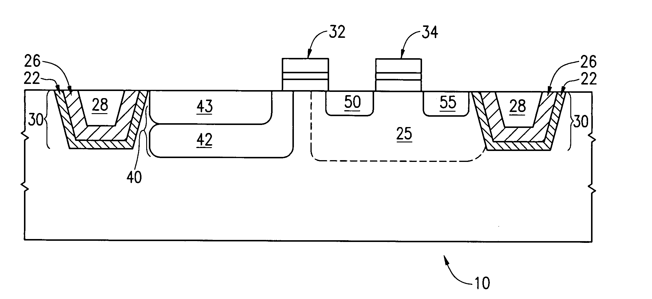
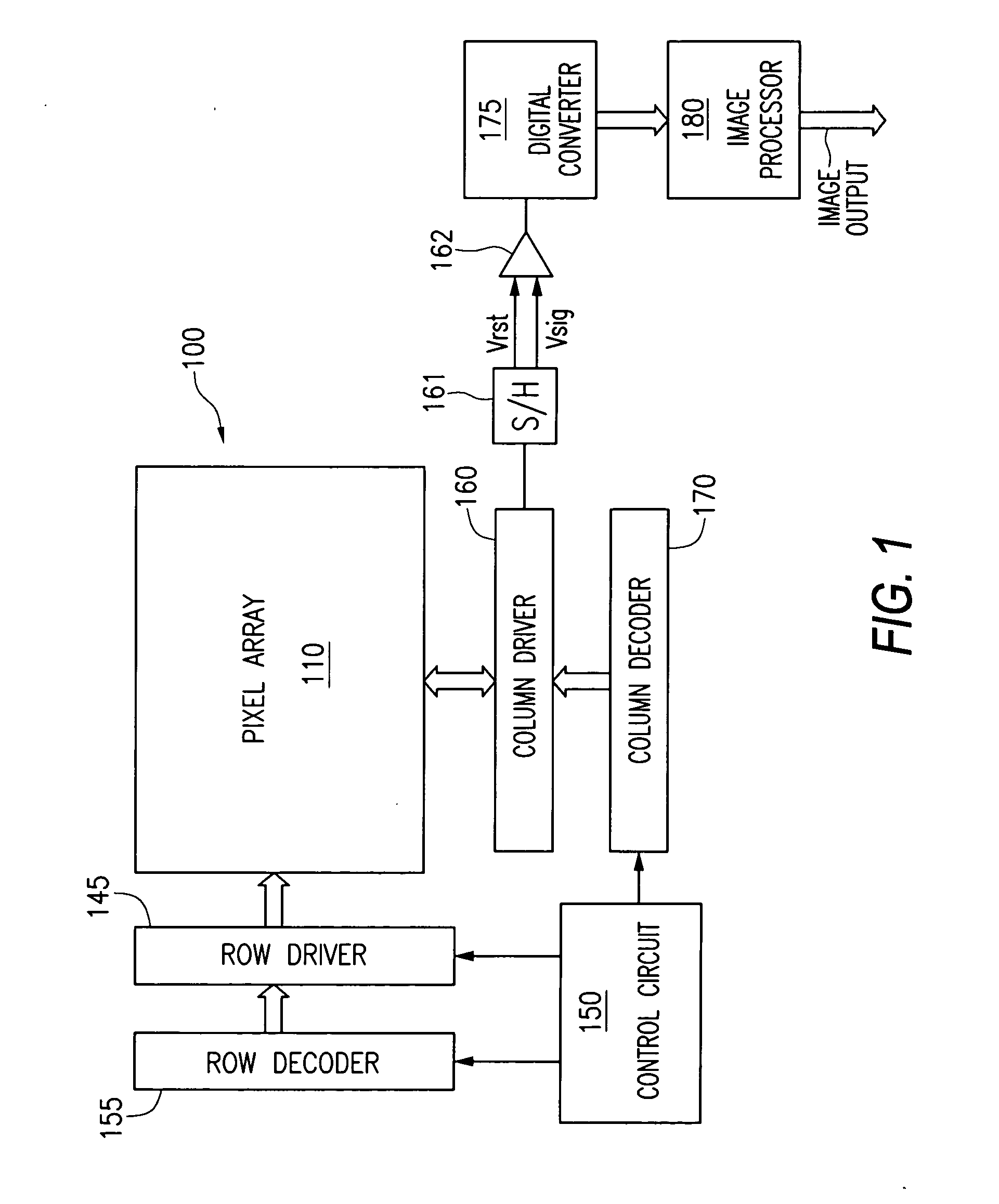
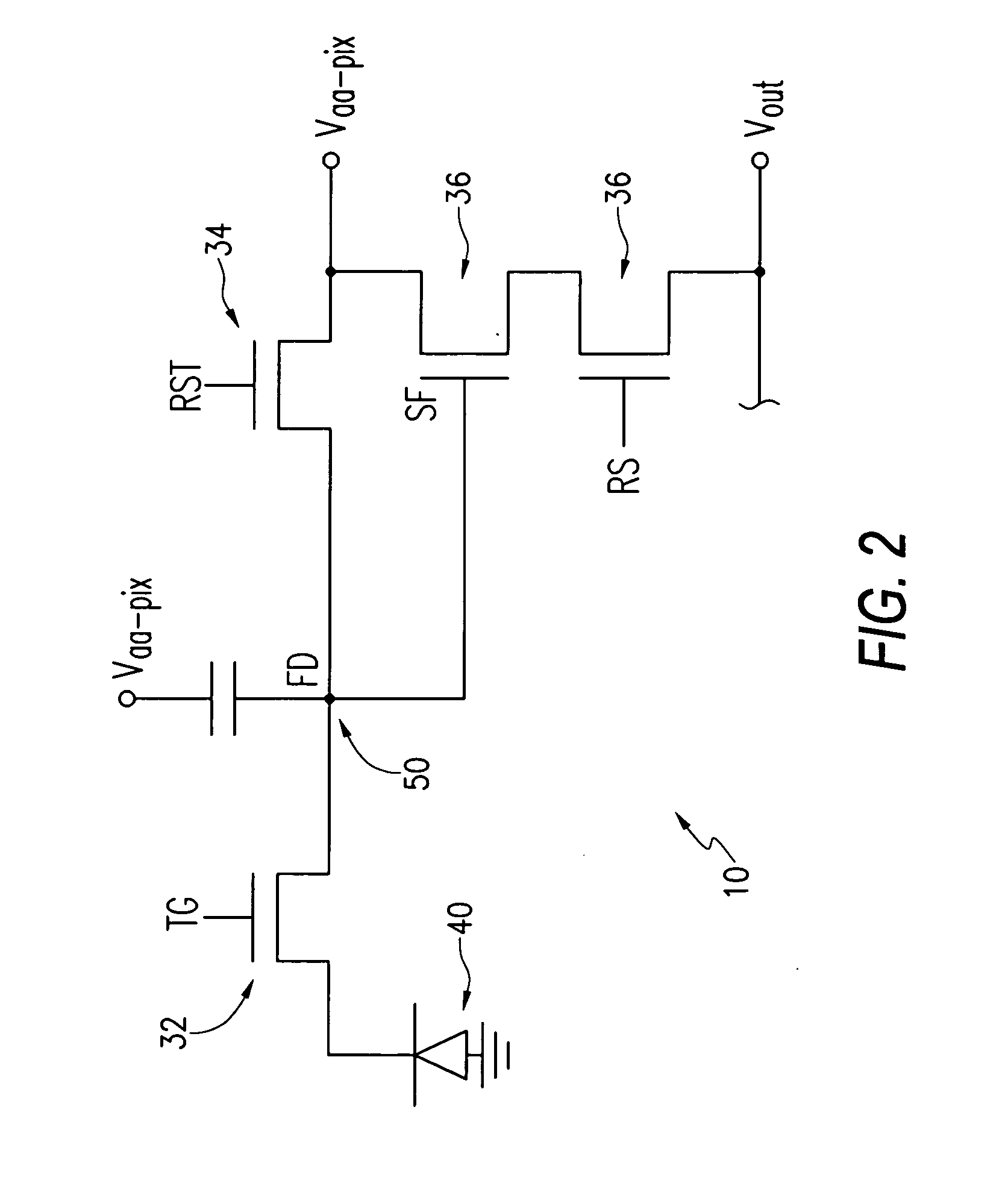
[0039] In the following detailed description, reference is made to the accompanying drawings which form a part hereof, and in which is shown by way of illustration specific embodiments in which the invention may be practiced. These embodiments are described in sufficient detail to enable those skilled in the art to practice the invention, and it is to be understood that other embodiments may be utilized, and that structural, logical and electrical changes may be made without departing from the spirit and scope of the present invention. Additionally, processing steps described and their progression are exemplary of preferred embodiments of the invention. However, the sequence of steps is not limited to that set forth herein and may be changed as is known in the art, with the exception of steps necessarily occurring in a certain order.

[0040] The term “substrate” is to be understood as a semiconductor-based material including silicon, silicon-on-insulator (SOI) or silicon-on-sapphire ...


PUM


Abstract

An imager device that has an isolation structure such that pinned photodiode characteristics are maintained without increasing doping levels. The invention provides an isolation structure to maintain pinned photodiode characteristics without increasing doping levels around the photodiode. By creating a substrate region surrounding the charge-collection region of the photodiode, the photodiode may be electrically isolated from the bulk substrate. This region fixes the depletion region so that it does not migrate toward the surface of the substrate or the STI region. By doing so, the region prevents charge from being depleted from the substrate and the accumulation region, reducing dark current.

Description

FIELD OF THE INVENTION [0001] The invention relates to the field of semiconductor devices and, in particular, to a pixel cell using a high-k dielectric film to create a strong accumulation region for providing isolation and optimizing characteristics of the cell. BACKGROUND OF THE INVENTION [0002] A CMOS imager circuit includes a focal plane array of pixel cells, each cell includes a photosensor, for example, a photogate, photoconductor or a photodiode overlying a substrate for producing a photo-generated charge in a doped region of the substrate. A readout circuit is provided for each pixel cell and includes at least a source follower transistor and a row select transistor for coupling the source follower transistor to a column output line. The pixel cell also typically has a floating diffusion node, connected to the gate of the source follower transistor. Charge generated by the photosensor is sent to the floating diffusion region. The imager may also include a transistor for tran...

Claims


Application Information

Patent Timeline
Patent Type & Authority Applications(United States)
IPC IPC(8): H01L21/8238H01L27/146H01L31/00H01L31/0352
CPCH01L27/1463H01L31/0352H01L27/14689H01L27/14643
Inventor MOULI, CHANDRA
Owner SAMSUNG ELECTRONICS CO LTD
Why Eureka
Try Eureka