Internal step-down power supply circuit

a power supply circuit and step-down technology, applied in the field of internal step-down power supply circuits, can solve the problems of inability to achieve compatibility with a follow-up to a change in internal step-down power supply potential, limited specs, etc., and achieve the effect of increasing current consumption and improving response performan

Inactive Publication Date: 2005-07-14
LAPIS SEMICON CO LTD
View PDF9 Cites 5 Cited by
  • Summary
  • Abstract
  • Description
  • Claims
  • Application Information

AI Technical Summary

Benefits of technology

[0005] An object of the present invention is to provide an internal step-down power supply circuit having a capability of improving response performance (transition from a standby state to an active state in particular) of a system without increasing current consumption.

Problems solved by technology

On the other hand, since the current that the amplifier can feed, is limited in terms of specs, various methods used up to now could not achieve compatibility with a follow-up to a change in internal step-down power-supply potential.

Method used


Image

  • Internal step-down power supply circuit
  • Internal step-down power supply circuit
  • Internal step-down power supply circuit

Examples


first embodiment

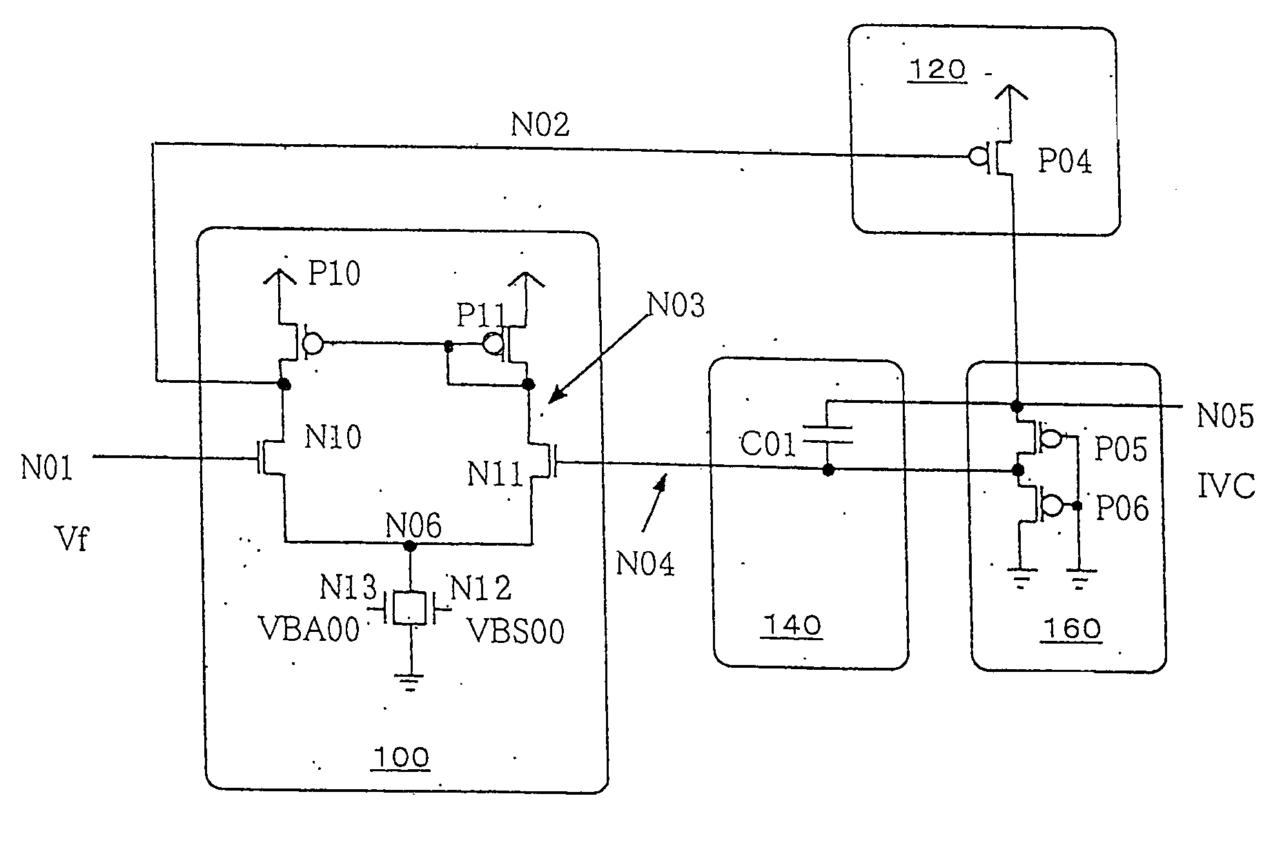
[0018]FIG. 1 is a circuit diagram showing an internal step-down power supply circuit of the present invention. In the present specification unless otherwise stated below, VDD indicates an external source or power supply voltage, IVC indicates an internal source or power-supply voltage indicative of a potential level lower than the level of the external power supply voltage VDD, “H” indicates an external source or power supply voltage level, “L” indicates a ground level, “VF” indicates a reference potential, and “VB” indicates a current control voltage for a differential amplifier, respectively. Further, NMOSs are signs indicative of N channel MOS transistors, PMOSs are signs indicative of P channel MOS transistors, CAPs are signs indicative of capacitors, INVs are signs indicative of inverters, respectively.

[0019] The internal step-down power supply circuit shown in FIG. 1, according to the first embodiment of the present invention comprises a differential amplifier 100, a driver 12...

second embodiment

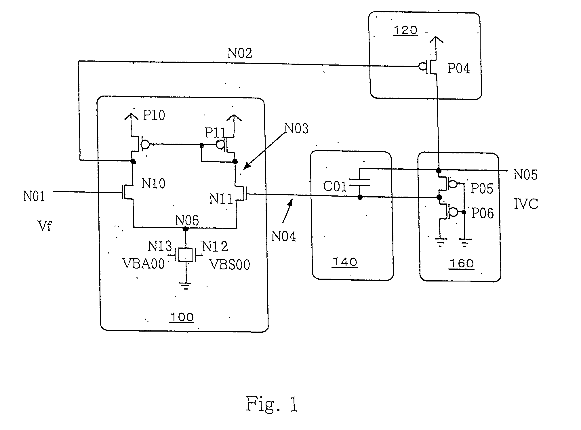
[0035]FIG. 2 is a circuit diagram showing an internal step-down power supply circuit according to the present invention. Incidentally, the same elements of structure as those in FIG. 1 are respectively identified by the same reference numerals in FIG. 2 and the description thereof will therefore be omitted.

[0036] Since the second embodiment is different from FIG. 1 in terms of a configuration of a differential amplifier 101, a description will be made of that portion alone.

[0037] The differential amplifier 101 comprises PMOSs P10 and P11, NMOSs N10, N11 and N22 through N25, and a stabilizing capacitor C20. In the differential amplifier 101, one electrode of the NMOS N10 is electrically connected to a node N02, the other electrode thereof is electrically connected to a node N26, and a gate electrode thereof is electrically connected to a node N01, respectively. One electrode of the NMOS N11 is electrically connected to a node N03, the other electrode thereof is electrically connecte...

third embodiment

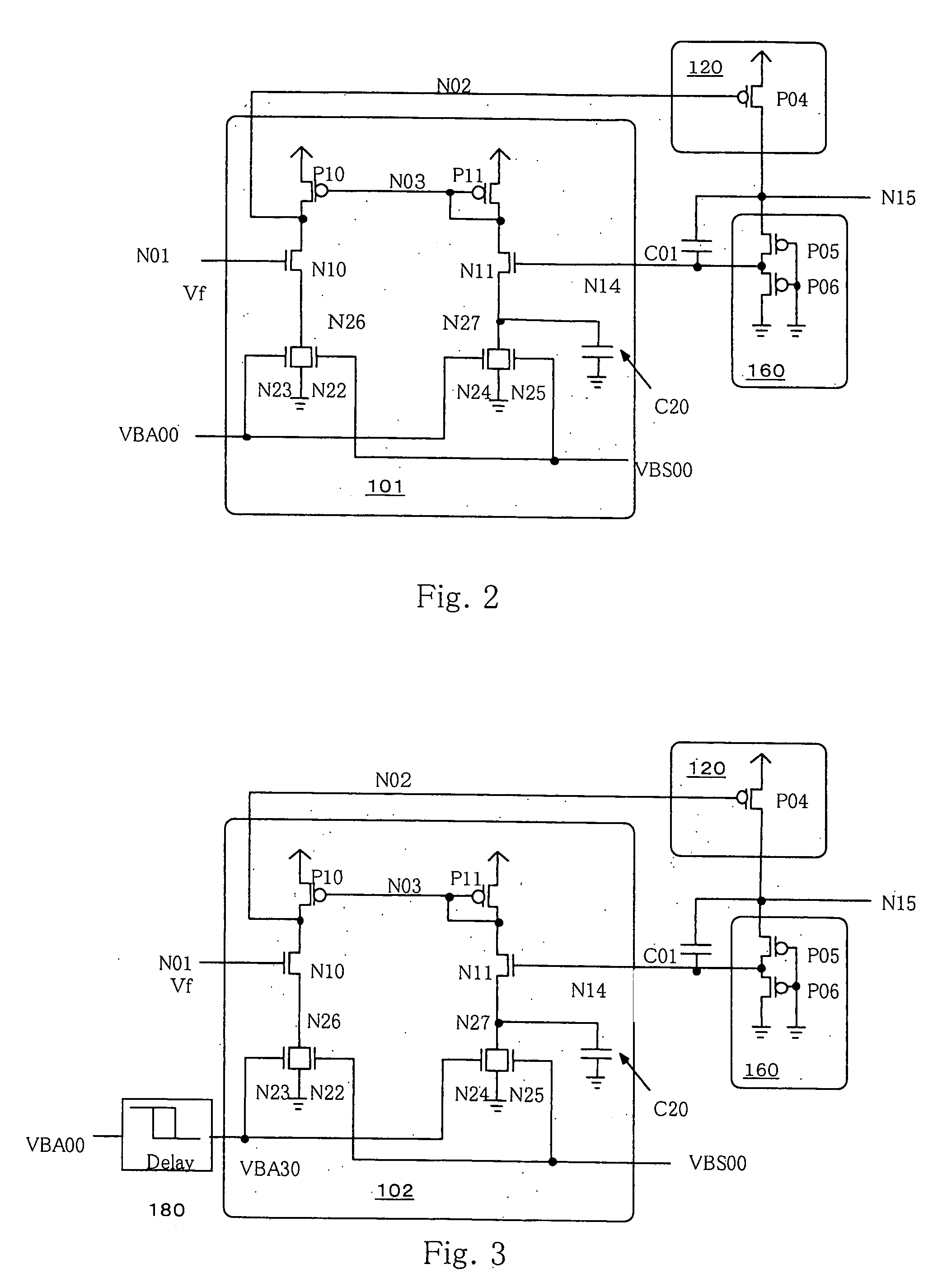
[0045]FIG. 3 is a circuit diagram showing an internal step-down power supply circuit according to the present invention. Incidentally, the same components as those shown in FIG. 2 are respectively identified by the same reference numerals in FIG. 3, and the description thereof will therefore be omitted.

[0046] The third embodiment is different in timing provided to input the signal VBA00 shown in FIG. 3. Namely, the third embodiment is provided with a delay circuit 180 for delaying the differential amplifier 102 employed in is the second embodiment from a standby state. Hence only portions associated with it will be described.

[0047] In a differential amplifier 102, gate electrodes of NMOSs N23 and N24 are respectively electrically connected to a node VBA30. The node VBA30 receives a signal VBA00 through the delay circuit 180 in such a manner that the signal VBA00 is delayed by a time required to completely bring an internal step-down power-supply slave circuit to the standby state u...


PUM


Abstract

An internal step-down power supply circuit has an internal step-down power-supply output node, a driver, a divider circuit and a current mirror circuit. The internal node provides an internal step-down power supply potential. The driver adjusts an external power-supply potential and provides an adjusted external power-supply potential to the internal node. The divider circuit divides a voltage that appears on the internal node and provides a divided voltage. The current mirror circuit is connected to the divider circuit. The current mirror circuit compares the voltage provided by the divider circuit and a reference voltage. The current mirror circuit sets the conductance of a first transistor feeding a current in response to the reference voltage to n times of the conductance of a second transistor feeding a current in response to the voltage provided from the divider circuit, wherein n is greater than 1.

Description

CROSS REFERENCE TO RELATED APPLICATIONS [0001] This is a divisional application of application Ser. No. 10 / 845,215, filed May 14, 2004, which is a divisional application of Ser. No. 10 / 243,644, filed Sep. 16, 2002, now U.S. Pat. No. 6,753,721, which are hereby incorporated by reference in their entirety for all purposes.BACKGROUND OF THE INVENTION [0002] The present invention relates to an internal step-down power supply circuit suitable for use in a semiconductor device. [0003] An internal step-down or deboost power supply circuit for generating an internal source or power-supply voltage by using an external power-supply voltage comprises a driver for supplying a source or power supply voltage, a divider circuit for dividing the internal power-supply voltage, an amplifier for comparing the voltage generated from the divider circuit and a reference voltage and supplying a drive voltage to the driver based on the result of comparison, etc. [0004] Now, the more a circuit connected to ...

Claims


Application Information

Patent Timeline
Patent Type & Authority Applications(United States)
IPC IPC(8): G11C11/413G05F1/46G05F1/56G11C11/407H01L21/822H01L27/04
CPCG05F1/465
Inventor OTSUKA, MASAYUKIHARADA, TERUHIRO
Owner LAPIS SEMICON CO LTD
Why Eureka
Try Eureka