Integrated electronic disconnecting circuits, methods, and systems

Active Publication Date: 2005-07-14
BOURNS INC
View PDF11 Cites 44 Cited by
  • Summary
  • Abstract
  • Description
  • Claims
  • Application Information

AI Technical Summary

Benefits of technology

[0009] Some embodiments use a gap between buried-layer diffusions to define the channel of the blocking transistor, which has the advantage of providing a high-breakdown-voltage device with good process integration capability.
[0010] Some embodiments use a gap between su

Problems solved by technology

It will be realized that implementing the circuit by soldering or otherwise connecting the discrete FETs results in a bulky device, which is less desirable.
Whil

Method used


Image

  • Integrated electronic disconnecting circuits, methods, and systems
  • Integrated electronic disconnecting circuits, methods, and systems
  • Integrated electronic disconnecting circuits, methods, and systems

Examples


Embodiment Construction

[0049] The numerous innovative teachings of the present application will be described with particular reference to the presently preferred embodiment (by way of example, and not of limitation).

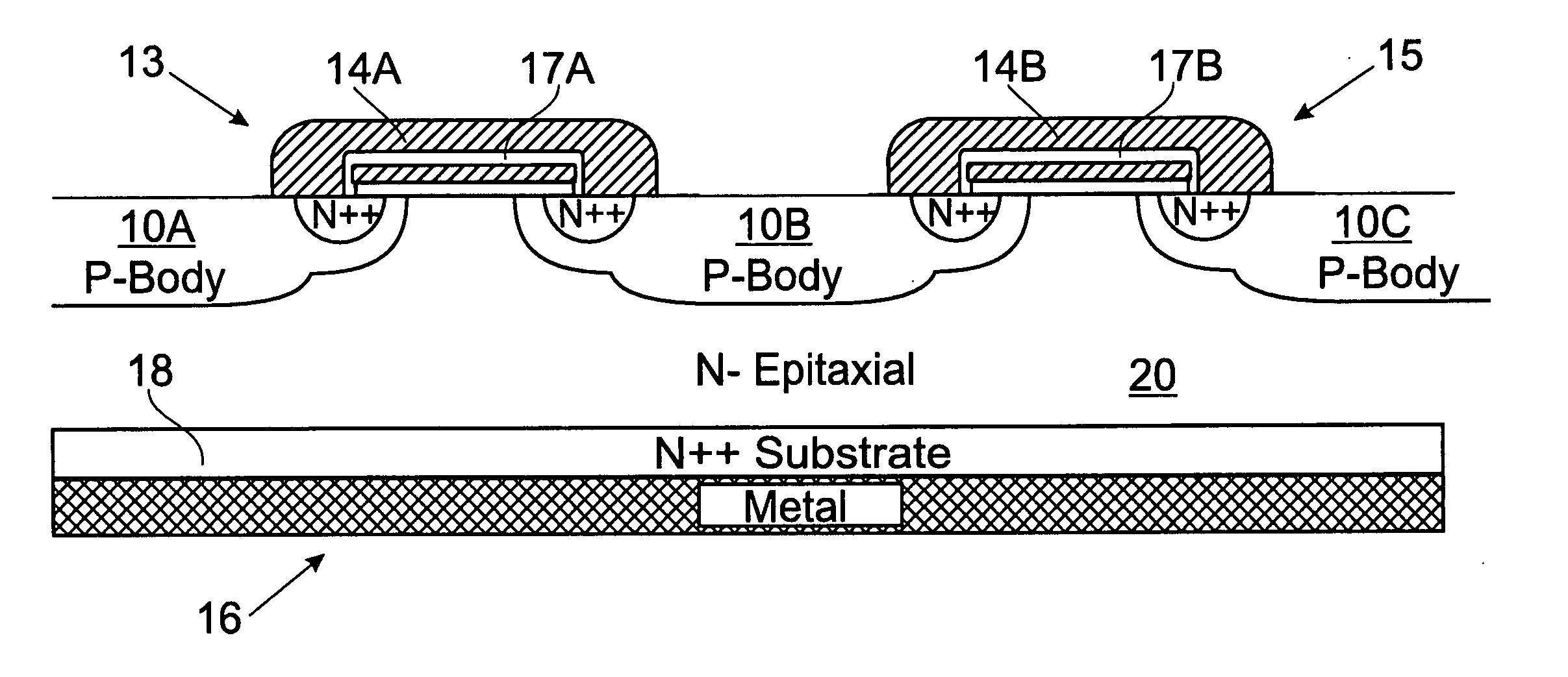
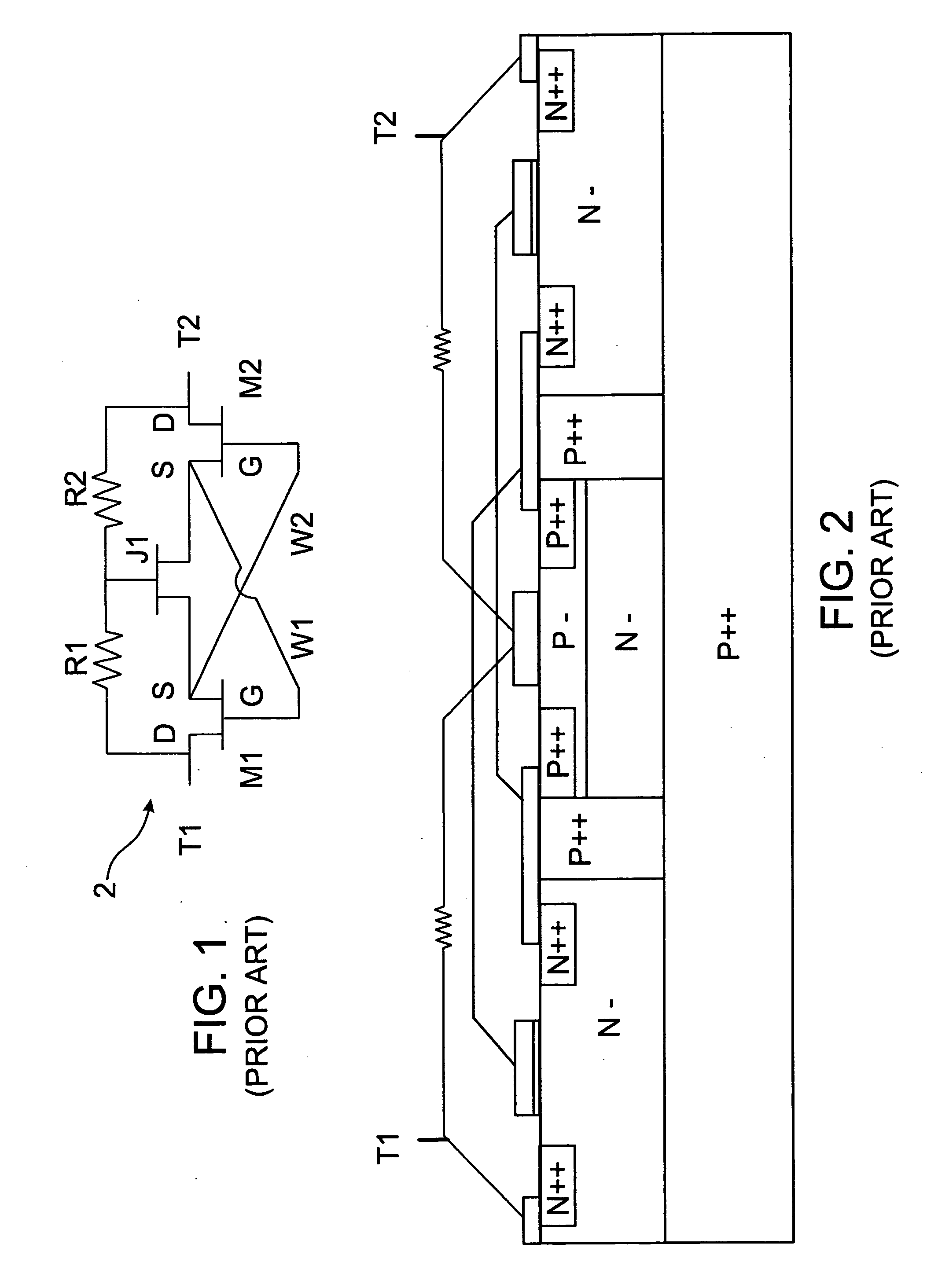
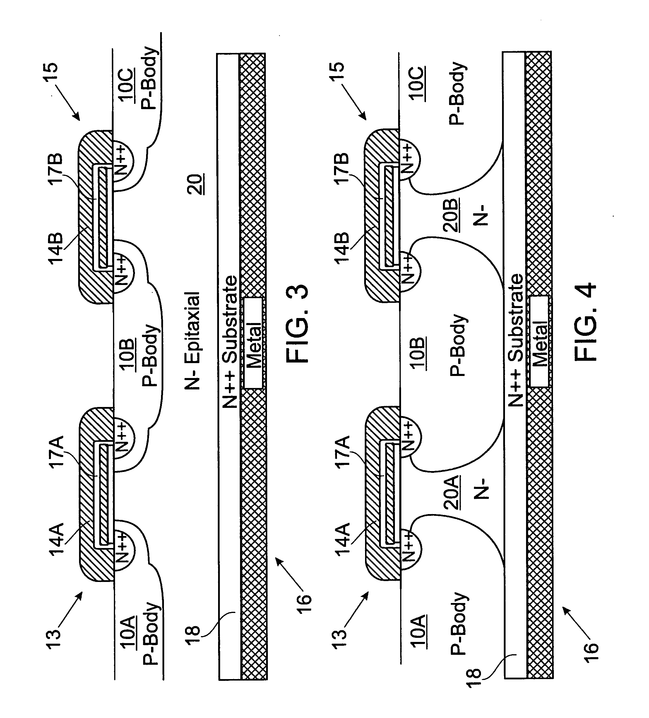
[0050]FIG. 1 is a circuit schematic of a protective circuit 2 according to an embodiment of international patent application PCT / AU94 / 00358 (WO 95 / 01667), which is hereby incorporated in its entirety by reference. The circuit includes two MOSFETs M1 and M2 in series connection with an intermediate JFET J1. Various feedback paths are provided by wires W1 and W2 and resistors R1 and R2.

[0051] MOSFETs M1 and M2 are typically fabricated according to a vertical channel design by which the drain and source are placed on opposite surfaces of a semiconductor wafer. An example of such a FET is described in U.S. Pat. No. 4,587,713 to Goodman et al, which is hereby incorporated by reference.

[0052] Other vertical channel FET designs are also known. For example, the first commercially available vertical...


PUM


Abstract

Merged devices for transient blocking. A pass transistor is placed so that its body potential drives the gate of a depletion-mode JFET-type blocking transistor. Thus a transient which appears on an external terminal is very rapidly propagated to shut off the blocking transistor, before large numbers of carriers can be injected. Preferably a shunt device is also used to drop high potentials which may appear at the same time. This connection can be particularly useful in power or data input terminals.

Description

CROSS-REFERENCE TO RELATED APPLICATIONS [0001] The present application claims priority from Australian provisional applications 2003904508, filed Aug. 21, 2003, and 2004901192, filed Mar. 9, 2004, both of which are hereby incorporated by reference. BACKGROUND AND SUMMARY OF THE INVENTION [0002] The present invention relates to a disconnecting circuit, and particularly to a solid-state device for blocking undesirable overvoltages and associated current transients from sensitive electronic circuitry. [0003] In international patent application WO 95 / 01667, which is hereby incorporated by reference, a series protective circuit is described. The protective circuit includes a number of discrete high voltage field effect transistors (FETs) and is placed in series between a power source and a load to be protected. The protective circuit is configured so that under normal conditions the drain-to-source resistance of the FETs assumes a low resistance state. However, in response to a high volt...

Claims


Application Information

Patent Timeline
IPC IPC(8): H01L27/098H01L29/06H01L29/08H01L29/10H01L29/78H01L29/808
CPCH01L27/098H01L29/0657H01L29/0696H01L29/8083H01L29/1095H01L29/7802H01L29/7827H01L29/0847
Inventor HARRIS, RICHARDLINEWIH, HANDOKO
Owner BOURNS INC
Why Eureka
Try Eureka