Protecting Silicon Germanium Sidewall with Silicon for Strained Silicon/Silicon Germanium MOSFETs

a silicon germanium and sidewall technology, applied in the direction of semiconductor devices, electrical apparatus, transistors, etc., can solve the problems of difficult to form epitaxial silicon, degrade the performance of devices and short channel immunity, and significant enhanced diffusion of dopants, so as to prevent adverse effects of ge and increase the active area

Inactive Publication Date: 2005-07-21
GLOBALFOUNDRIES INC
View PDF12 Cites 14 Cited by
  • Summary
  • Abstract
  • Description
  • Claims
  • Application Information

AI Technical Summary

Benefits of technology

[0010] The raised source and drain regions thus include one or more silicon layers on sidewalls of the source and drain regions. The silicon prevents adverse effects of Ge during silicidation, including Ge out diffusion and silicide line breakage. The Si also increases the active area.

Problems solved by technology

One problem with this technique is that epitaxial growth must take place at temperatures as high as 750° C., which may cause significant transient enhanced diffusion of dopants.
The unnecessary dopant redistribution in halo / extension regions degrades the performance of devices and short channel immunity.
Moreover, with a very thin SOI film, it can be difficult to form epitaxial silicon without causing silicon agglomeration due to possible contamination of carbon in certain chemical vapor deposition tools.
Unfortunately, however, Ge degrades silicide contact formation and contact resistance due to its inherent function as a diffusion barrier.
Another problem with raised silicon / silicon germanium source and drain regions involves contact formation.
However, this process is generally not as effective with semiconductor materials other than silicon.
For example, a cobalt silicide contact formed to a source disposed in a strained Si layer and an underlying SiGe layer may form a high-resistivity compound in the SiGe layer, thereby compromising the functionality of the contact.

Method used


Image

  • Protecting Silicon Germanium Sidewall with Silicon for Strained Silicon/Silicon Germanium MOSFETs
  • Protecting Silicon Germanium Sidewall with Silicon for Strained Silicon/Silicon Germanium MOSFETs
  • Protecting Silicon Germanium Sidewall with Silicon for Strained Silicon/Silicon Germanium MOSFETs

Examples


Embodiment Construction

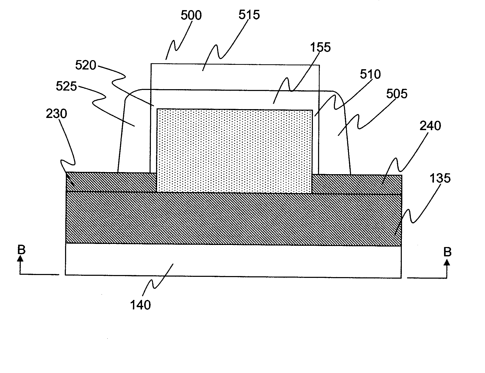
[0016] The invention enables fabrication of raised Si / SiGe source and drain regions with epitaxially grown silicon on SiGe sidewalls. The silicon prevents adverse effects of Ge during silicidation, including Ge out diffusion and silicide line breakage. The Si also increases the active area.

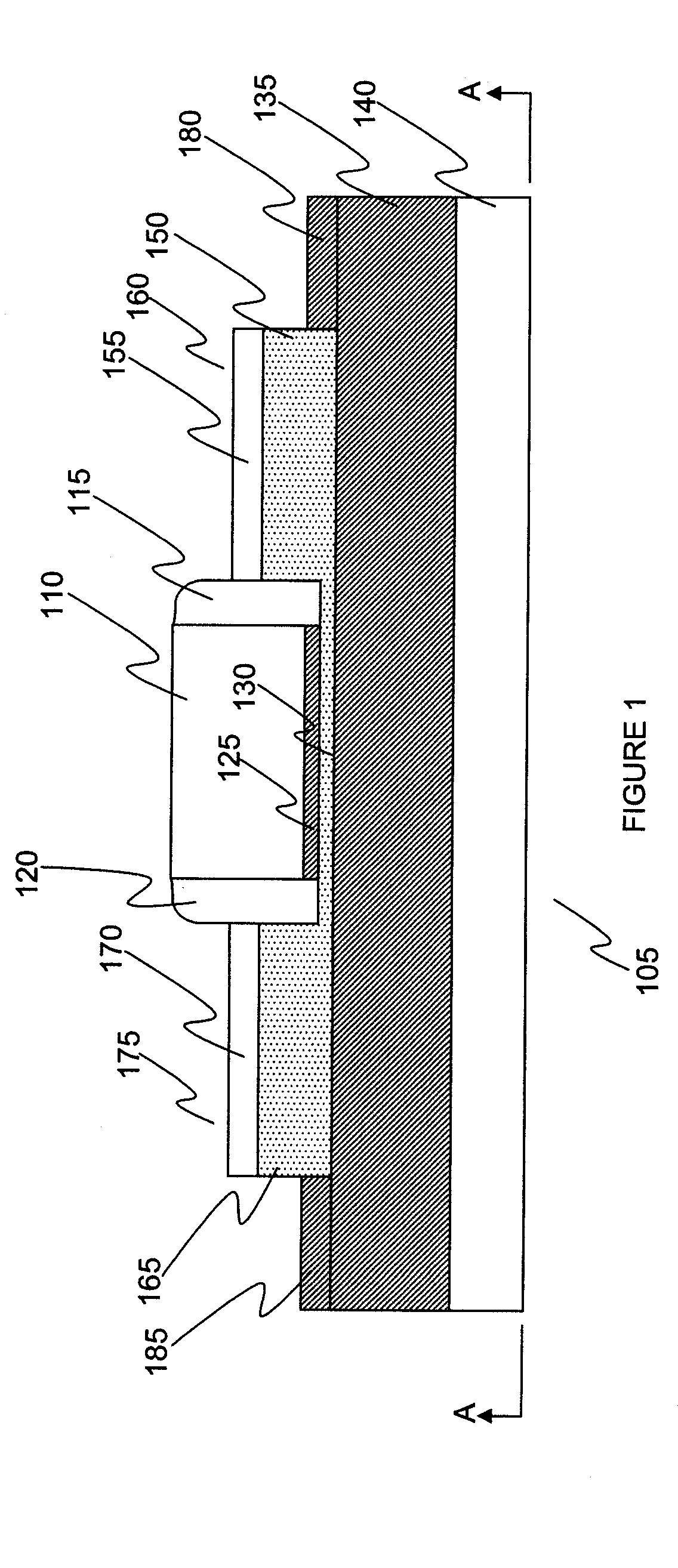
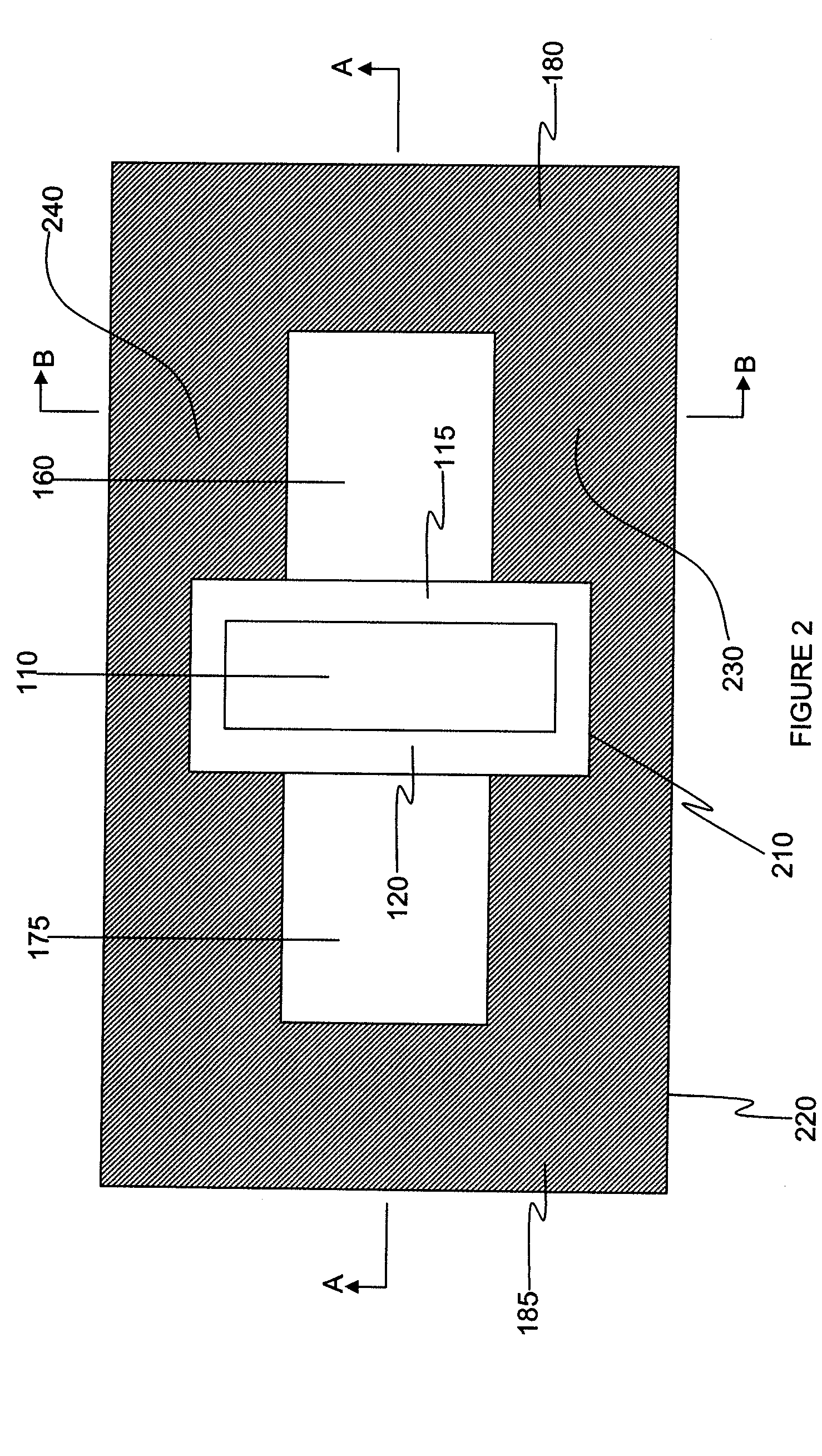
[0017] Referring to FIG. 1, an exemplary initial structure employed in the invention is shown. Specifically, the exemplary initial structure is comprised of an SOI substrate 105 having a patterned gate stack region 110 formed on the surface thereof. The SOI substrate 105 may include a buried oxide layer 125 sandwiched between a top Si-containing layer 130 and a bottom Si-containing layer 140. The top Si-containing layer 130 is an area upon which devices may be formed. The Si-containing layer 130 may be comprised of various semiconducting materials that include silicon, such as Si, SiGe, SiC, SiGeC, Si / Si, or Si / SiGe.

[0018] The SOI substrate 105 employed in the present invention may be fabricated...


PUM


Abstract

Raised Si/SiGe source and drain regions include epitaxially grown silicon on SiGe sidewalls. The epi silicon prevents adverse effects of Ge during silicidation, including Ge out diffusion and silicide line breakage. The Si also increases the active area.

Description

BACKGROUND OF INVENTION [0001] The invention generally relates to a semiconductor device and method of manufacture and, more particularly, to a semiconductor device that includes strained silicon / silicon germanium field effect transistors with a protective silicon layer. [0002] As silicon film thickness of Silicon On Insulator (SOI) is reduced, for high-performance CMOS fabrication, it becomes necessary to increase the thickness of source / drain regions above the SOI thickness. This results from the fact that, as the SOI film becomes thinner, a reduced amount of Si material is available from which to form silicide for source / drain contacts. Additionally, thinner source / drain regions can degrade on-current due to increased series resistance. [0003] To maintain or reduce overall source / drain series resistance, including the silicide contact resistance, techniques have emerged to form raised source / drain (RSD) structures. For example, selective epitaxial growth of silicon has been used ...

Claims


Application Information

Patent Timeline
Patent Type & Authority Applications(United States)
IPC IPC(8): H01L21/336H01L29/06H01L29/10H01L29/78H01L29/786
CPCH01L29/1054H01L29/66628H01L29/66772H01L29/78654H01L29/7842H01L29/78618H01L29/7834
Inventor ZHU, HUILONGDORIS, BRUCE B.MOCUTA, DAN M.
Owner GLOBALFOUNDRIES INC
Why Eureka
Try Eureka