Light-emitting device with enlarged area of active luminescence region

Inactive Publication Date: 2005-07-21
OPTO TECH
View PDF4 Cites 17 Cited by
  • Summary
  • Abstract
  • Description
  • Claims
  • Application Information

AI Technical Summary

Benefits of technology

[0007] For this purpose, how to design a novel light-emitting device with not only a relatively enlarged area of active luminescence region in a LED in order to enhance the brightness, but also

Problems solved by technology

On the contrary, when the current density flowing through the active luminescence region is so low that the luminous yield could not be fully developed, the area of the element may be wasted.
Therefore, how to facilitate the working current to flow through the active luminescence region 153 uniformly for enhancing the lumin

Method used


Image

  • Light-emitting device with enlarged area of active luminescence region
  • Light-emitting device with enlarged area of active luminescence region
  • Light-emitting device with enlarged area of active luminescence region

Examples


Example

[0029] The structural features and the effects to be achieved may further be understood and appreciated by reference to the presently preferred embodiments together with the detailed description.

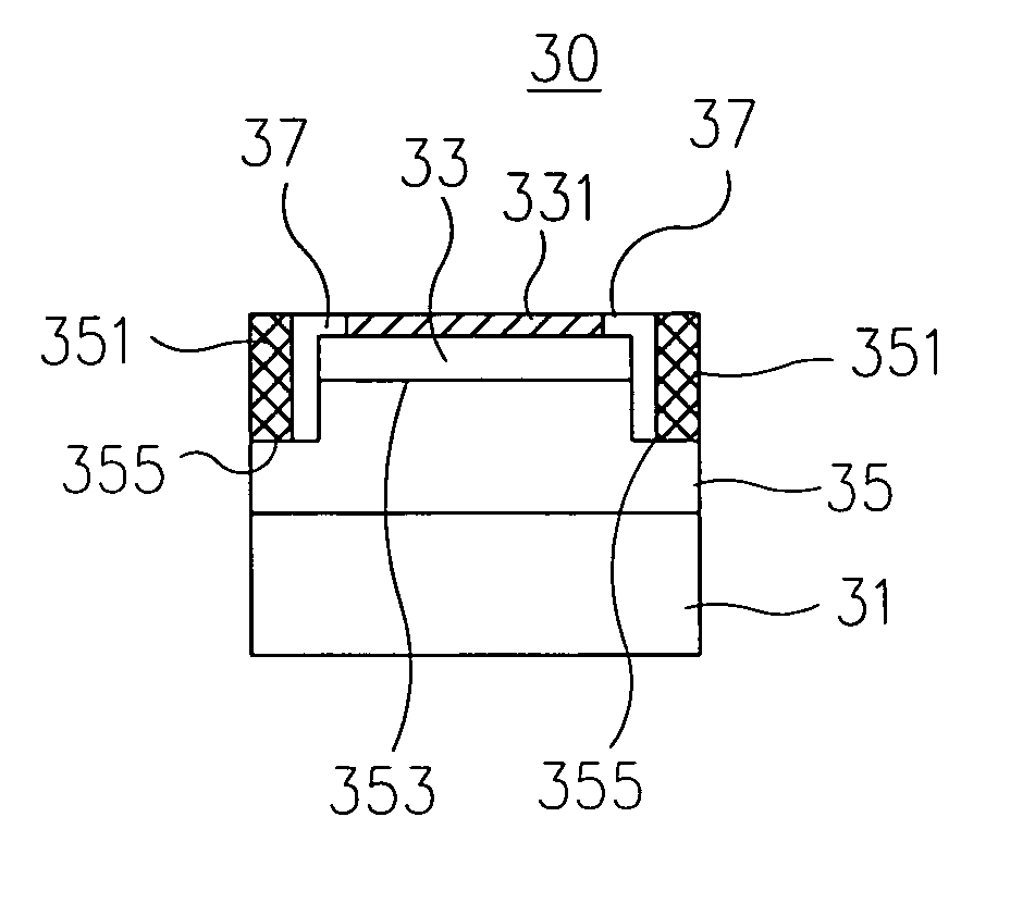
[0030] Referring to FIGS. 3A to 3C, firstly, there are shown a top view of the structure according to one preferred embodiment of the present invention, a cross section view taken along line C-D in FIG. 3A, and a top view of the structure of a power supply substrate. As illustrated in these figures, a light-emitting diode (LED) device with an enlarged active luminescence region essentially comprises a LED die 30 and a power supply substrate 41, in which the LED die 30 is mainly formed with, on a die substrate 31, a second epitaxy layer 35 defining a relatively projecting first surface 353 and a relatively recessed second surface 355, and the first surface 353 is further formed with a first epitaxy layer 33 thereon, such that an active luminescence region (i.e., first surface 353) may be for...


PUM


Abstract

A light-emitting device is provided, having an enlarged area of active luminescence region to enhance the brightness, mainly comprising a second epitaxy layer and at least one first epitaxy layer provided on a die substrate in turn. On the top surface of the first epitaxy layer, there are provided with at least one first electrode, and a plurality of second electrodes passing through the first epitaxy layer, insulated with the first epitaxy layer by means of an electrode insulation layer, and electrically connected to the second epitaxy layer, in which the first electrode and the second electrodes are alternately arranged. Moreover, first power supply circuits and second power supply circuits are provided on a power supply substrate at positions based on the locations of the first electrode and second electrodes so as to be adhesively electrically connected to the first electrode and the second electrodes, correspondingly. The plurality of first power supply circuits is connectedly provided with a first connective circuit, and the second power supply circuits are connectedly provided with a second connective circuit. The first connective circuit and second connective circuit are provided on the power supply substrate, instead of provided on the light-emitting device directly. Thus, the area of active luminescence region is relatively enlarged, whereby the luminous yield is enhanced accordingly.

Description

FIELD OF THE INVENTION [0001] The present invention is related to a light-emitting device, particularly to a light-emitting device having an enlarged area of active luminescence region so as to enhance the brightness, essentially providing a first connective circuit and a second connective circuit on a power supply substrate, without occupying the active luminescence region of the light-emitting device directly. BACKGROUND [0002] Light-emitting devices (LEDs) have been widely used in computer peripherals, communication products, and other electronic equipments owing to advantages, such as small volume, light weight, lower power consumption, and long service life, as examples. For general mass-produced LEDs, there is grown an epitxy layer with a PN junction on a substrate, made from the material such as sapphire, SiC, and so on. The light may be projected from the PN junction owing to the recombination of electron-hole, when a drive voltage is applied across two sides of the P-type e...

Claims


Application Information

Patent Timeline
IPC IPC(8): H01L27/15H01L29/26H01L29/267H01L31/0203H01L31/0352H01L31/12H01L33/08H01L33/20H01L33/38
CPCH01L33/08H01L33/38H01L33/20
Inventor LIN, MING-DERLIN, SAN BAOHSU, JUNG-KUEI
Owner OPTO TECH
Why Eureka
Try Eureka