
Analog buffer and method for driving the same

a buffer and analog technology, applied in the field of analog buffers, can solve the problems of difficult miniaturization and simplifying the lcd, the thinness and weight of thin film type flat panel display devices, and the inability to form tfts directly on the glass substrate of the lcd, so as to improve the color picture display and reduce power consumption

Inactive Publication Date: 2005-07-21
LG DISPLAY CO LTD
View PDF2 Cites 14 Cited by
  • Summary
  • Abstract
  • Description
  • Claims
  • Application Information

AI Technical Summary

Benefits of technology

[0026] Another object of the present invention is to provide an analog buffer having low power consumption.
[0027] Another object of the present invention is to provide an analog buffer that improves a color picture display.
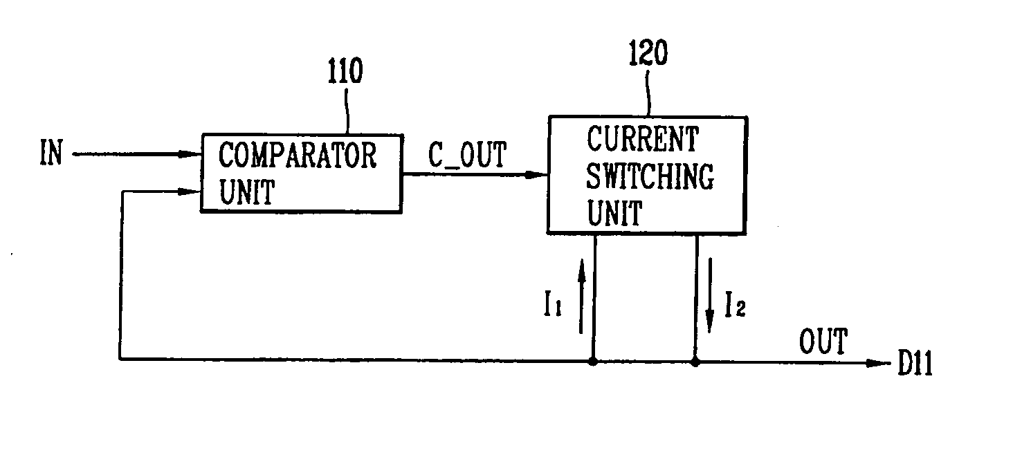
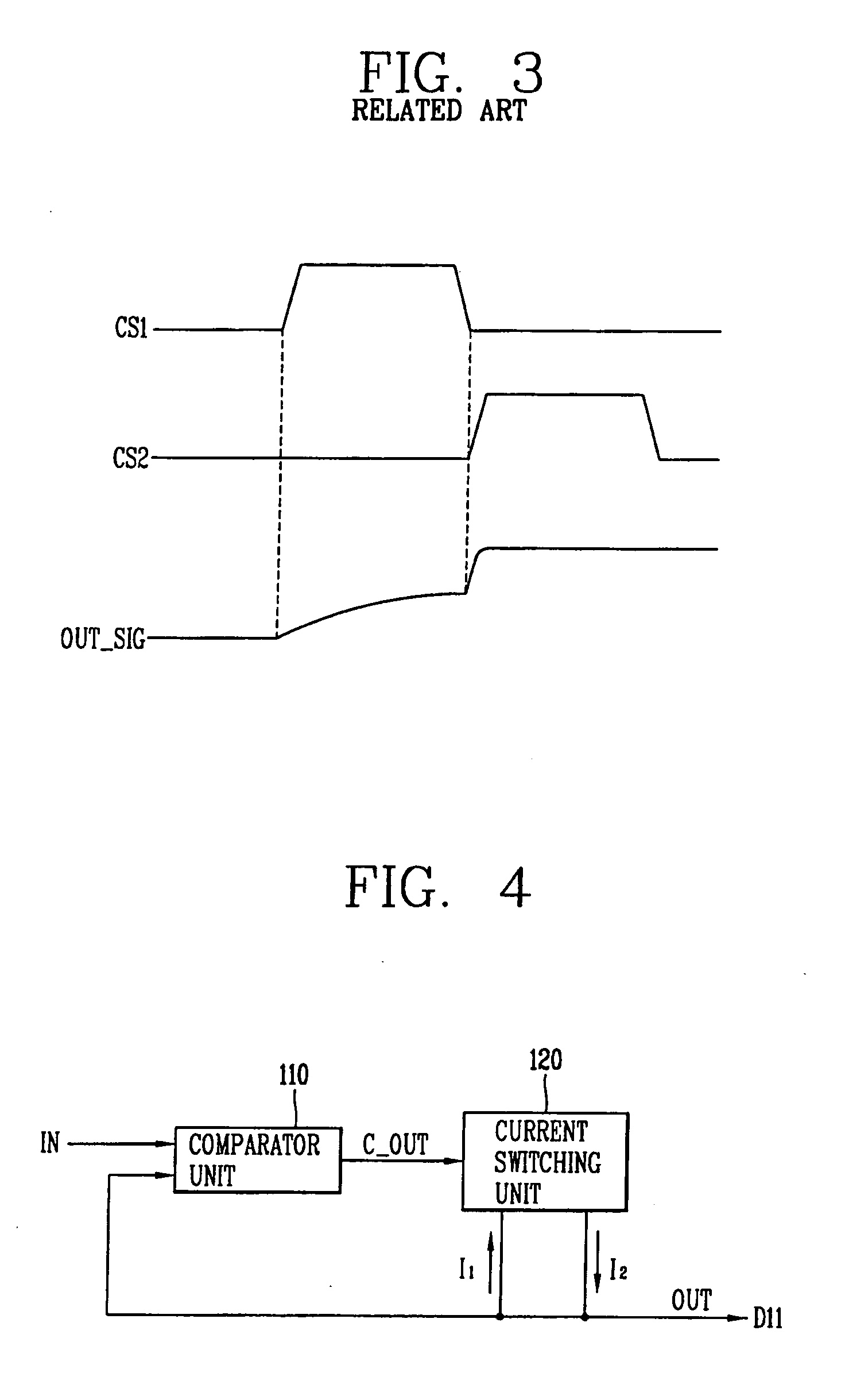
[0029] To achieve these and other advantages and in accordance with the purpose of the present invention, as embodied and broadly described, an analog buffer includes a comparator unit for comparing an input signal to be charged on a signal line of a display panel with an output signal charged on the signal line of the display panel to output a control signal; and a current switching unit for discharging an output current from the signal line of the display panel or charging an input current on the signal line of the display panel in accordance with the control signal output by the comparator unit the comparator unit smallest and to thus minimize leakage current.
[0032] In another aspect, a method of driving an analog buffer includes comparing an input signal to be charged on a signal line of a display panel with an output signal charged on the signal line of the display panel; discharging an output current from the signal line of the display panel or charging an input current on the signal line of the display panel in accordance with a result of comparing the input signal with the output signal; correcting a level of the output signal which is higher than a desired level; and stopping a charge or discharge of a leakage current.

Problems solved by technology

In general, among flat panel display devices for displaying images, thin film type flat panel display devices are thin and lightweight.
However, since polycrystalline silicon is formed by high temperature fabrication processes, it is not possible to form the TFTs directly on the glass substrate of the LCD.
Thus, it is difficult to miniaturize and to simplify the LCD.
Moreover, as the number and the length of wiring lines for transmitting driving signals increase in larger displays, various noises and electromagnetic interference (EMI) are generated.
Therefore, the reliability of larger displays deteriorates and manufacturing cost increases.
However, the load of the data lines and the gate lines can increase such that it is not possible to apply the desired signals in a short enough time.
However, since the transistors made of polycrystalline silicon can have large differences in electrical characteristics, the operational amplifier designed with the polycrystalline silicon transistors has a large offset voltage and a large amount of power is consumed by static current such that the operational amplifier made of polycrystalline silicon transistors cannot be used as the analog buffer.
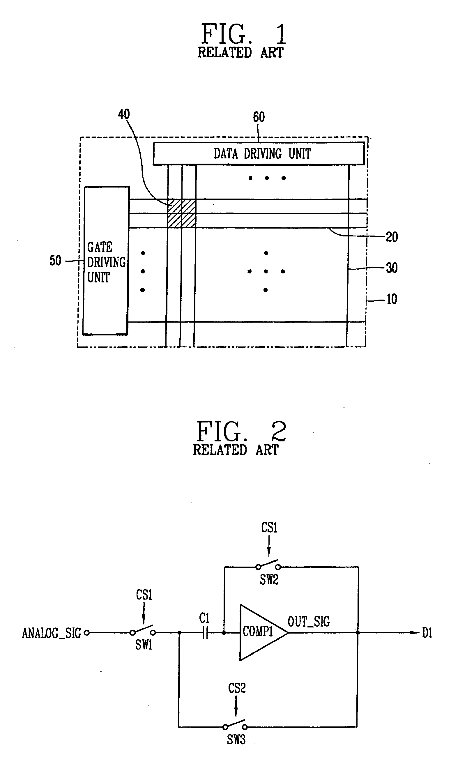
In the case of a high resolution and large area LCD in which the load of the data line D1 connected to the output port of the comparator COMP1 is large, the size of the comparator COMP1 must be increased, thereby increasing leakage current and power consumption.

Method used


Image

  • Analog buffer and method for driving the same
  • Analog buffer and method for driving the same
  • Analog buffer and method for driving the same

Examples


Embodiment Construction

[0045] Reference will now be made in detail to the preferred embodiments of the present invention, examples of which are illustrated in the accompanying drawings.

[0046]FIG. 4 is a block diagram illustrating an exemplary analog buffer according to an embodiment of the present invention. Referring to FIG. 4, the analog buffer includes a comparator unit 110 and a current switching unit 120. The comparator unit 110 compares an input signal IN to be charged on a data line D11 of a display panel with an output signal OUT charged on the data line D1 of the display panel to output a control signal C_OUT. In response to the control signal C_OUT, the current switching unit 120 discharges a current I1 from the data line D11 or charges a current I2 on the data line D11.

[0047]FIG. 5 is an exemplary circuit diagram of an analog buffer according to an embodiment of the present invention. Referring to FIG. 5, the comparator unit 110 includes a first comparator COMP11 and a second comparator COMP1...


PUM


Abstract

An analog buffer includes a comparator unit for comparing an input signal to be charged on a signal line of a display panel with an output signal charged on the signal line of the display panel to output a control signal; and a current switching unit for discharging an output current from the signal line of the display panel or charging an input current on the signal line of the display panel in accordance with the control signal output by the comparator unit the comparator unit smallest and to thus minimize leakage current.

Description

[0001] The present invention claims the benefit of Korean Patent Application No. 2003-100826, filed in Korea on Dec. 30, 2003, which is hereby incorporated by reference. BACKGROUND OF THE INVENTION [0002] 1. Field of the Invention [0003] The present invention relates to an analog buffer, and more particularly, to an analog buffer for a flat panel display device. [0004] 2. Discussion of the Related Art [0005] In general, among flat panel display devices for displaying images, thin film type flat panel display devices are thin and lightweight. The thin film type flat panel display devices have been recently developed because of their versatility. In particular, they are used in high resolution and high reaction speed liquid crystal display devices (LCD) that are capable of displaying moving pictures. [0006] LCD devices use the optical anisotropy of liquid crystal molecules to transmit or block light transmission. Liquid crystal molecules transmit or block light depending unpon their o...

Claims


Application Information

Patent Timeline
IPC IPC(8): G09G3/36G02F1/133
CPCG09G3/3685G09G2300/0408G09G2330/021G09G2310/0291G09G2310/0272G02F1/133
Inventor KIM, KEE-JONG
Owner LG DISPLAY CO LTD
Learn More