

Using protective cups to fabricate light emitting semiconductor packages
a technology of light-emitting semiconductors and protective caps, which is applied in the direction of applications, other domestic articles, coatings, etc., can solve the problems of solid material, high cost operation, and use of mems devices
- Summary
- Abstract
- Description
- Claims
- Application Information
AI Technical Summary
Benefits of technology
Problems solved by technology
Method used
Image

Examples
Embodiment Construction
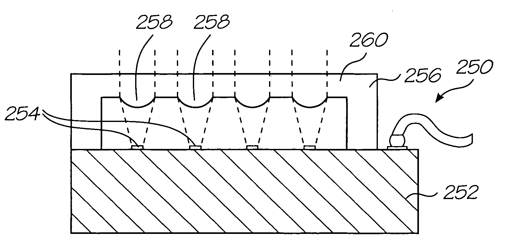
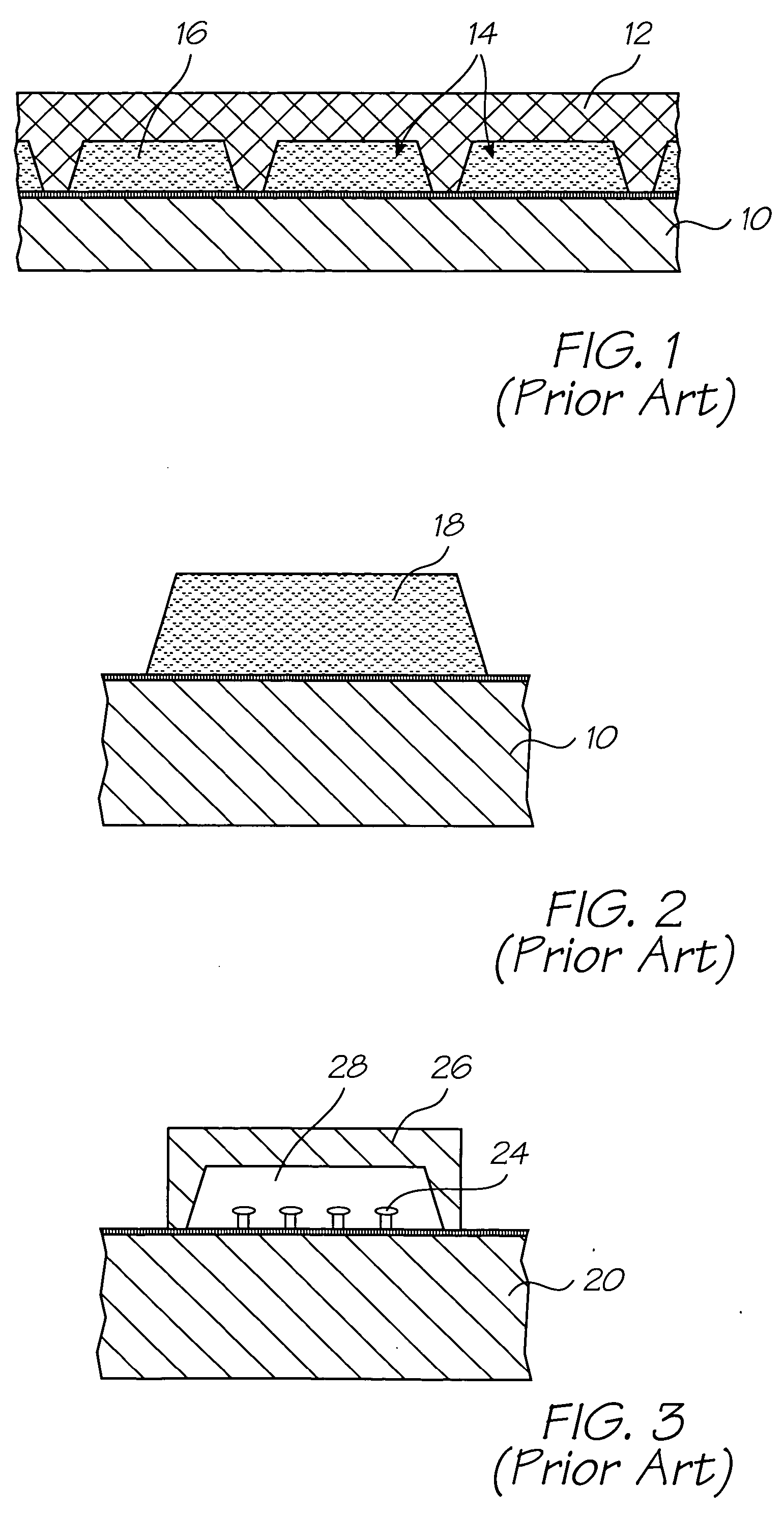
[0042] Referring to FIGS. 1 and 2 there is show a prior art method of forming protective caps on semiconductor wafers on a wafer scale. A semiconductor wafer 10 is clamped against a mold 12 having cavities 14 formed therein and a liquid polymer material 16 is injected into the cavities 14. The polymer material sets to form solid protective caps 18. The wafer is then singulated using a wafer saw. This technique is not applicable to wafers having MEMS devices formed thereon as the liquid polymer material will surround the MEMS devices and stop them from working.
[0043]FIG. 3 shows the present prior art technique for protecting MEMS devices. The MEMS chip 20 including the MEMS devices 24, shown symbolically, is bonded to a silicon wafer 26. This may be carried out at the individual chip stage or at the wafer stage. The wafer 26 is typically etched using a crystallographic anisotropic etch using an etchant such as KOH to form a series of recesses 28 which correspond to the locations of ...
PUM
| Property | Measurement | Unit |
|---|---|---|
| thickness | aaaaa | aaaaa |
| thickness | aaaaa | aaaaa |
| thickness | aaaaa | aaaaa |
Abstract
Description
Claims
Application Information