Method and structure for eliminating polarization instability in laterally - oxidized VCSELs
- Summary
- Abstract
- Description
- Claims
- Application Information
AI Technical Summary
Benefits of technology
Problems solved by technology
Method used
Image
Examples
Embodiment Construction
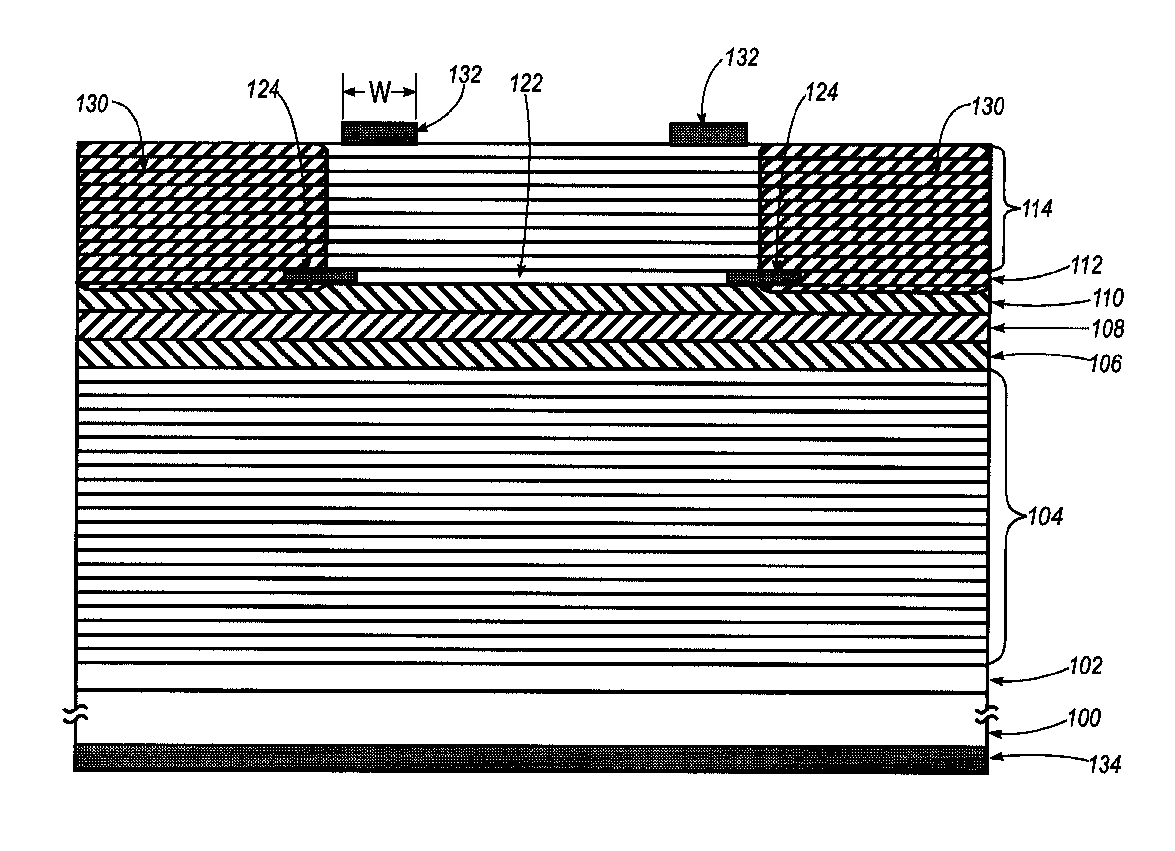
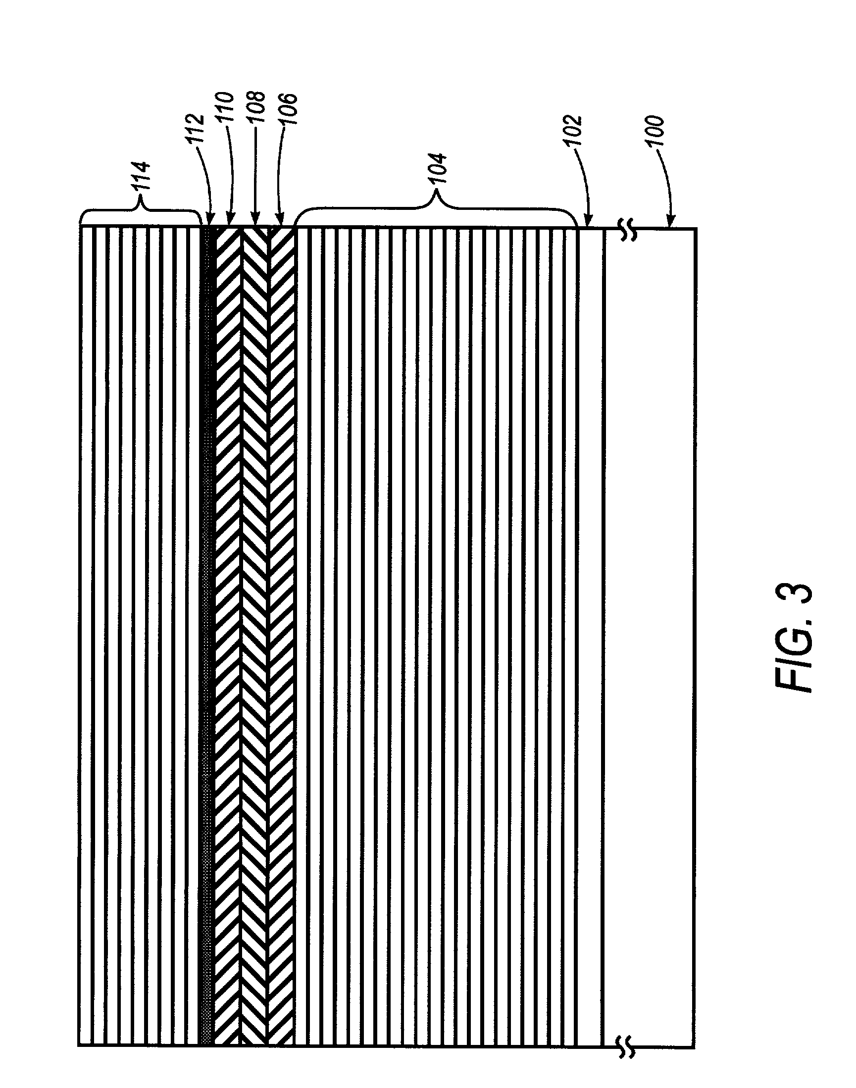
[0044]FIG. 3 illustrates a semiconductor structure which is used to form the preferred embodiment of the present invention. The structure illustrated includes a number of semiconductor layers, which can be used to form a vertical cavity surface emitting laser. As will be apparent, the layers are illustrated schematically only and bear no relationship to the relative thicknesses each to the other. As shown in FIG. 3, an n-type GaAs buffer layer 102 of approximately 200 nanometers is grown on an n-type GaAs substrate 100 using an epitaxial deposition process known as metal-organic chemical vapor deposition (“MOCVD”). The doping level of the n-type GaAs substrate and GaAs buffer are typically around the range of 3×1018 cm−3 to 7×1018 cm−3 so that a reasonably low resistance can be achieved in these layers. The semiconductor layers may also be deposited on a substrate by liquid phase epitaxy (“LPE”), molecular beam epitaxy (“MBE”), or other known crystal growth processes.
[0045] Above t...
PUM
 Abstract
Description
Claims
Application Information


