Alignment method, method for manufacturing a semiconductor device, substrate for a semiconductor device, electronic equipment

a semiconductor device and alignment method technology, applied in the direction of instruments, photomechanical devices, optics, etc., can solve the problems of inability to correctly align with the underlying semiconductor film, and difficulty in making an alignment based on the pattern on the surface of the film, so as to achieve high performance and high accuracy of alignment

Inactive Publication Date: 2005-07-28
SEIKO EPSON CORP
View PDF10 Cites 37 Cited by
  • Summary
  • Abstract
  • Description
  • Claims
  • Application Information

AI Technical Summary

Benefits of technology

[0007] In consideration of this problem, the invention can provide an alignment method that is preferably applicable when manufacturing equipments by liquid-phase processing. The alignment method can include the following steps in a device manufacturing process including forming of a functional film on a substrate by liquid-phase processing, forming an alignment mark on the substrate on which the functional film is formed so as to make a pattern of the alignment mark appear on a film that is formed after forming the functional film, and aligning the film that is formed after forming the functional film by using the alignment mark. Using the alignment mark can provide accurate patterning of a film that is formed after forming the functional film.
[0029] Electronic equipment of the invention can also include a semiconductor device manufactured by any of the above-mentioned methods for manufacturing a semiconductor device. This method can provide high performance electronic equipment.

Problems solved by technology

While manufacturing such devices, however, the planarization of surface of their films may cause a problem.
Therefore, if a film that does not transmits light is formed on the thin film for patterning, it can be difficult to make an alignment based on the pattern on the surface of the film like in photo processing.
For example, if the gate insulating film or interlayer insulating film of a thin-film transistor is formed by liquid-phase processing, the surface of a metal film formed on the insulating film has no concave-convex pattern, and thereby it cannot be correctly aligned with an underlying semiconductor film.

Method used


Image

  • Alignment method, method for manufacturing a semiconductor device, substrate for a semiconductor device, electronic equipment
  • Alignment method, method for manufacturing a semiconductor device, substrate for a semiconductor device, electronic equipment
  • Alignment method, method for manufacturing a semiconductor device, substrate for a semiconductor device, electronic equipment

Examples


first embodiment

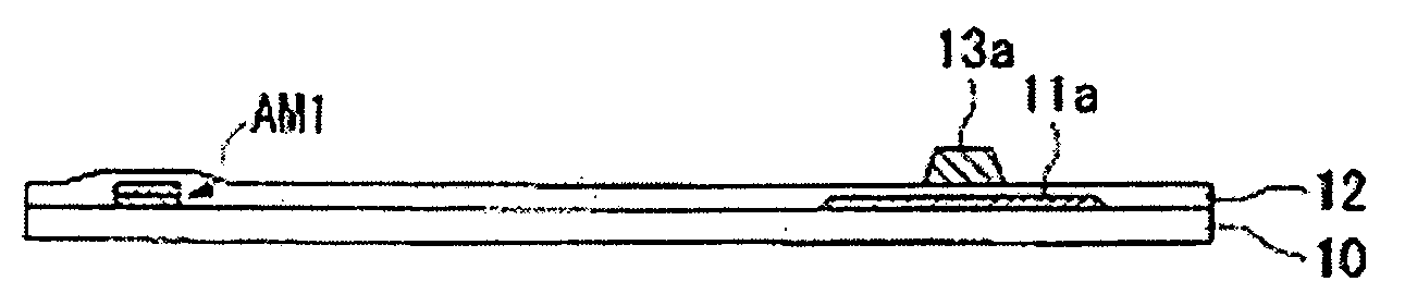
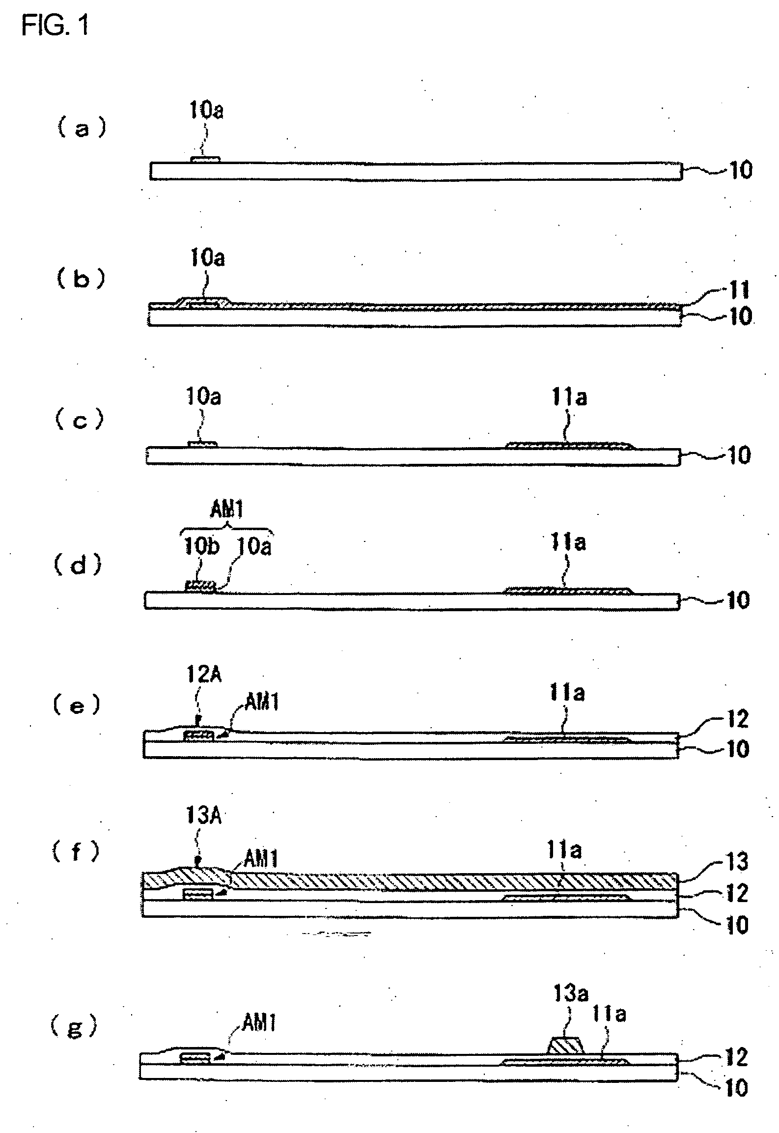
[0070] Referring now to FIGS. 3 and 4, a second exemplary embodiment of the invention will be described. FIGS. 3 and 4 are process drawings illustrating a method for manufacturing a TFT which is an example of semiconductor devices according to the exemplary embodiment. The drawings schematically show a transistor forming region and an alignment mark forming region in a magnified form. In this embodiment, the same members and elements as those in the first embodiment will be given the same reference numerals, and further description thereof will be omitted.

[0071] The substrate 10 having the alignment mark (first alignment mark) 10a, as shown in FIG. 3a, is provided as a substrate for manufacturing a semiconductor device (substrate for a semiconductor device). On the substrate 10, a semiconductor film made of amorphous silicon or the like is deposited as shown in FIG. 3b. Then the semiconductor film is crystallized by laser annealing, for example, and isolated by etching, for example....

fourth embodiment

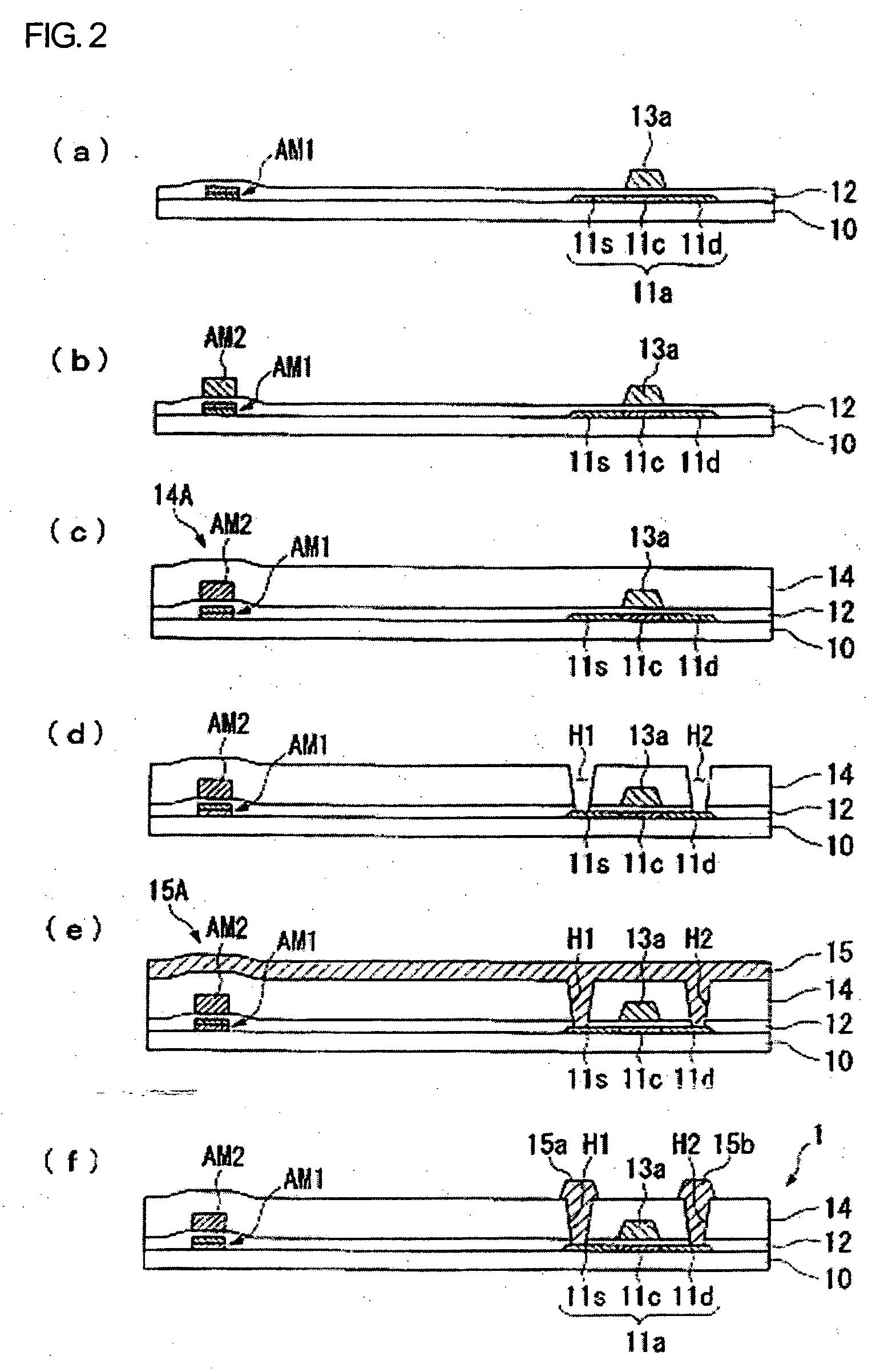
[0142] Referring now to FIG. 9, a sixth exemplary embodiment of the invention will be described. FIG. 9 is a process drawing illustrating a method for manufacturing a TFT according to the present embodiment. The drawing is a sectional view schematically showing the TFT forming region (element area) E1 and the alignment mark forming region (alignment area) E2 in a magnified form. In this embodiment, the same members and elements as those in the third or fourth embodiment will be given the same reference numerals, and further description thereof will be omitted.

[0143] On the substrate 110, a semiconductor film made of amorphous silicon or the like is formed. Then the semiconductor film is crystallized by laser annealing, for example, and patterned by etching, for example. As shown in FIG. 9a, this process forms the amorphous semiconductor film (first semiconductor film) 111a having a predetermined shape in the element area E1, and also forms the second semiconductor film 111b serving ...


PUM


Abstract

Aspects of the invention can provide an alignment method that is preferably applicable when manufacturing equipments by liquid-phase processing. The alignment method in a device manufacturing process can include forming of a functional film on a substrate by liquid-phase processing, forming an alignment mark on the substrate on which the functional film is formed so as to make a pattern of the alignment mark appear on a film that is formed after forming the functional film, and aligning the film that is formed after forming the functional film by using the alignment mark.

Description

BACKGROUND [0001] 1. Technical Field of Invention [0002] Aspects of the invention can relate to an alignment method, a method for manufacturing a semiconductor device, a substrate for a semiconductor device, and electronic equipment. [0003] 2. Description of Related Art [0004] Related art methods for manufacturing a thin-film electronic device have been developed based on vacuum processing employing evaporation. While the vacuum processing can provide extremely high processing accuracy, it consumes a significant amount of energy and materials ineffectively. Therefore, low energy consuming, liquid-phase processing (using a liquid-phase method) has come under review as a substitution for the vacuum processing. See, for example, Domestic Republication of PCT International Publication No. WO 00 / 59040. [0005] The liquid-phase processing provides the following advantages over the related art vacuum processing that involves evaporation. First, no vacuum equipment is required, which makes i...

Claims


Application Information

Patent Timeline
Patent Type & Authority Applications(United States)
IPC IPC(8): H01L29/786H01L21/00H01L21/027H01L21/208H01L21/31H01L21/336H01L21/68H01L21/76H01L21/77H01L21/84H01L23/544
CPCH01L23/544H01L29/66757H01L2223/54453H01L27/1292H01L2924/0002H01L2924/00G03F7/2028H01L27/1214
Inventor YUDASAKA, ICHIOTANAKA, HIDEKI
Owner SEIKO EPSON CORP
Why Eureka
Try Eureka