Light-emitting diode structure with electrostatic discharge protection

a technology of led structure and protection circuit, which is applied in the direction of semiconductor devices, semiconductor/solid-state device details, electrical apparatus, etc., can solve the problems of increasing the overall packaging time and cost of led structure with conventional electrostatic discharge protection circuit, easy damage by abnormal voltage or electrostatic discharge,

Inactive Publication Date: 2005-08-04
EPISTAR CORP
View PDF2 Cites 114 Cited by
  • Summary
  • Abstract
  • Description
  • Claims
  • Application Information

AI Technical Summary

Benefits of technology

[0010] The present invention is related to a LED structure having electrostatic discharge (ESD) protection function in which a shunt diode is connected in parallel to the LED with an inverse voltage compared to the LED. Therefore, the LED can be protected from the damage due to electrostatic discharge.

Problems solved by technology

It is noted that, although LED has so many advantages described above, however, the disadvantages of the LED is that it gets easily damaged by an abnormal voltage or electrostatic discharge (ESD).
However, when an abnormal voltage or electrostatic charge is generated, the over level high voltage is discharged by the Zener diode 40 that operates in the breakdown region.
However, the process of fabricating the circuit structure is complicated as it requires a number of additional process steps, such as, the step of forming the P-type doped silicon 44 in the N-type doped silicon 42 requiring expensive apparatus, namely, an ion implanter, related gas supporting devices and vacuum system.
Accordingly, the overall packaging time and cost of the LED structure having conventional electrostatic discharge (ESD) protection circuit are increased.

Method used


Image

  • Light-emitting diode structure with electrostatic discharge protection
  • Light-emitting diode structure with electrostatic discharge protection
  • Light-emitting diode structure with electrostatic discharge protection

Examples


Embodiment Construction

[0026] The present invention now will be described more fully hereinafter with reference to the accompanying drawings, in which preferred embodiments of the invention are shown. This invention may, however, be embodied in many different forms and should not be construed as limited to the embodiments set forth herein; rather, these embodiments are provided so that this disclosure will be thorough and complete, and will fully convey the scope of the invention to those skilled in the art. Like numbers refer to like elements throughout.

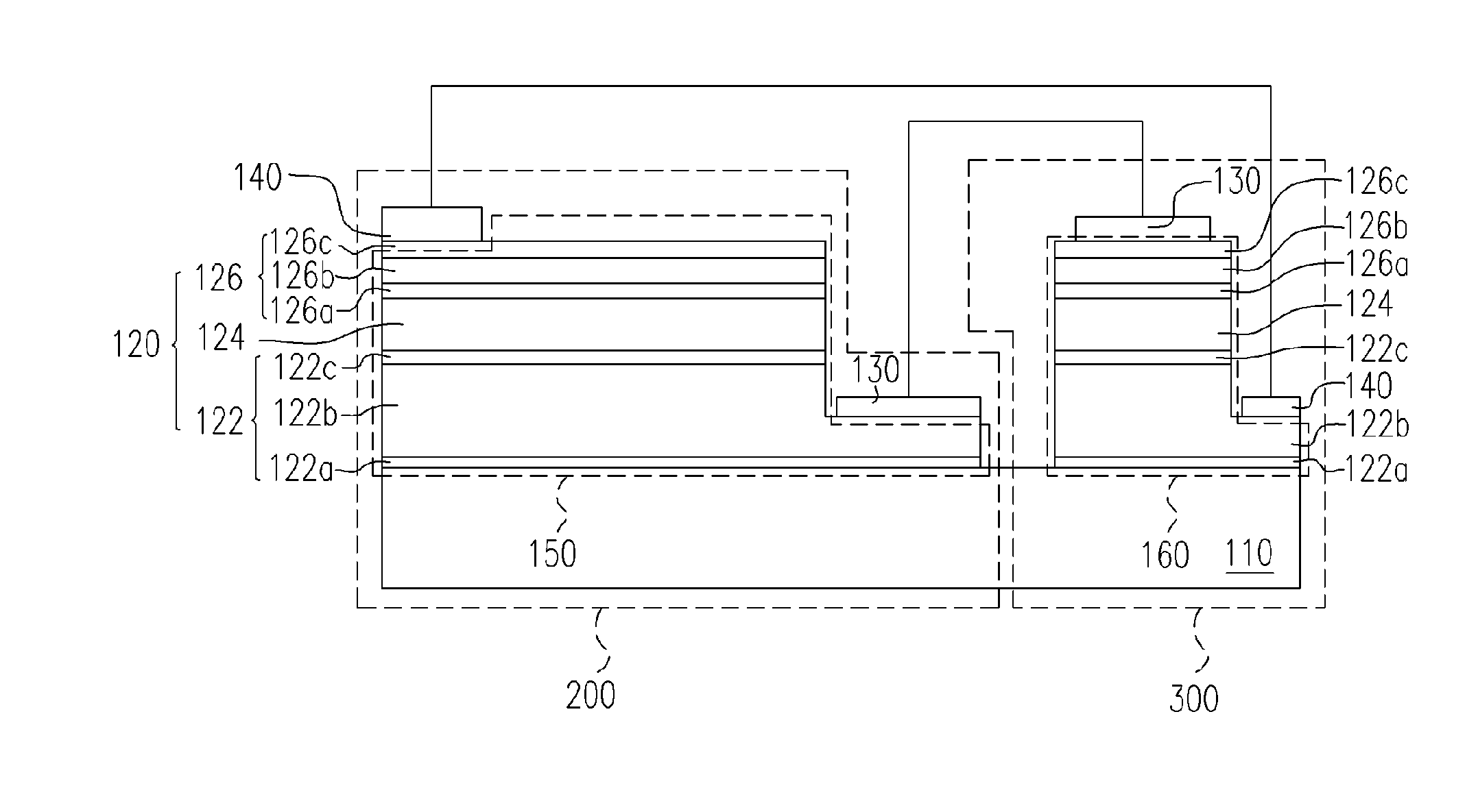
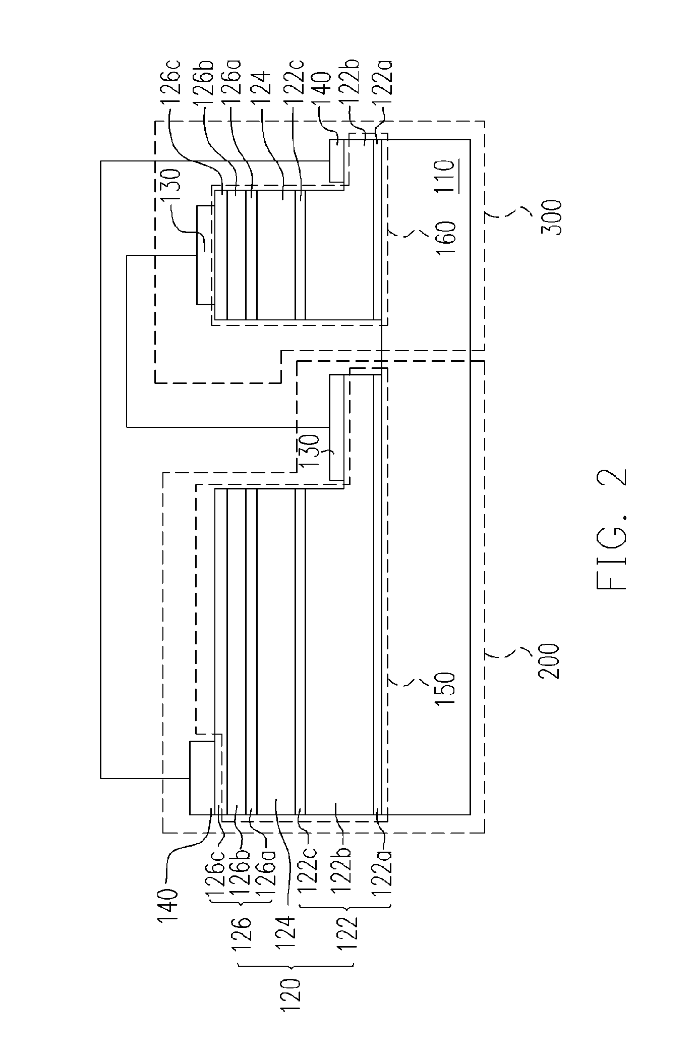
[0027]FIG. 2 is a cross-sectional view schematically illustrating a LED including electrostatic discharge (ESD) protection function according to one embodiment of the present invention. Referring to FIG. 2, the LED includes, for example but not limited to, a substrate 110, a patterned semiconductor layer 120, a first electrode 130 and a second electrode 140. The patterned semiconductor layer 120 is disposed over the substrate 110. The patterned semicondu...


PUM


Abstract

A light-emitting diode (LED) structure with electrostatic discharge (ESD) protection is described. The LED includes a substrate, a patterned semiconductor layer, a first electrode and a second electrode. The patterned semiconductor layer is disposed over the substrate, and is divided into at least a first island structure and a second island structure. The first electrode and the second electrode are connected between the first island structure and the second island structure. A shunt diode is formed by the first electrode, the second electrode and the second island structure. The shunt diode is connected in parallel to the LED with an inverse voltage compared to the LED. In the LED structure of the invention, the first island structure and the second island structure are manufactured simultaneously by the epitaxy procedure. Therefore, the LED could be protected from damage due to electrostatic discharge (ESD).

Description

CROSS-REFERENCE TO RELATED APPLICATION [0001] This application claims the priority benefit of Taiwan application serial no. 93102264, filed Feb. 2, 2004. BACKGROUND OF THE INVENTION [0002] 1. Field of the Invention [0003] The present invention generally relates to a light emitting diode (LED) and a method thereof. More particularly, the present invention relates to a LED structure having electrostatic discharge (ESD) protection function. [0004] 2. Description of Related Art [0005] In general, light emitted by a light emitting diode (LED) comprising a III-V compound semiconductor material has a wide bandgap of emitting light covering almost all the wavelength range of infrared (IR), ultra-violet (UV) and visible light. For a LED device, the internal quantum efficiency and the external quantum efficiency (or so-called light extraction efficiency) are two important parameters. Conventionally, the method of increasing the internal quantum efficiency is to improve the crystal quality of ...

Claims


Application Information

Patent Timeline
Patent Type & Authority Applications(United States)
IPC IPC(8): H01L25/16H01L27/15H01L33/00
CPCH01L25/167H01L27/15H01L23/62H01L2924/0002H01L2924/00
Inventor SHEI, SHIH-CHANGSHEU, JINN-KONG
Owner EPISTAR CORP
Why Eureka
Try Eureka