Power plane system of high-speed digital circuit for suppressing ground bounce noise

a digital circuit and power plane technology, applied in cross-talk/noise/interference reduction, electronic switching, pulse technique, etc., can solve the problems of significant signal integrity (si) problem and electromagnetic interference (emi), capacitor parasitic inductance, and suppression effect will decrease, so as to achieve efficient suppression of electromagnetic radiation and break the stop-band bandwidth

Active Publication Date: 2005-08-04
NAT SUN YAT SEN UNIV
View PDF5 Cites 17 Cited by
  • Summary
  • Abstract
  • Description
  • Claims
  • Application Information

AI Technical Summary

Benefits of technology

[0012] According to the invention, when the ground bounce noise occurs, the metal units can broaden the stop-band bandwidth. Therefore, the signals in the stop-band a...

Problems solved by technology

The resonance mode excited by the ground bounce noise causes significant signal integrity (SI) problem and electromagnetic interference (EMI) issues.
Nevertheless, in the...

Method used


Image

  • Power plane system of high-speed digital circuit for suppressing ground bounce noise
  • Power plane system of high-speed digital circuit for suppressing ground bounce noise
  • Power plane system of high-speed digital circuit for suppressing ground bounce noise

Examples


first embodiment

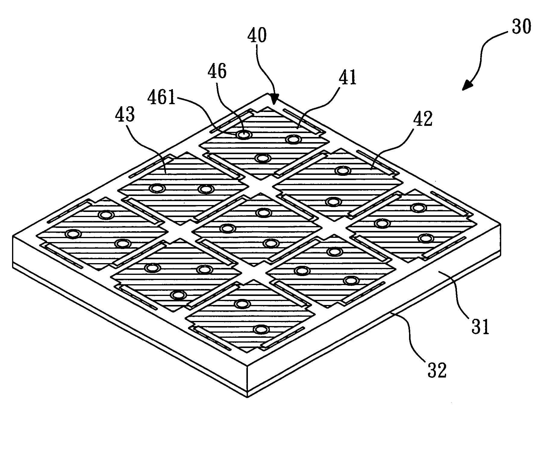
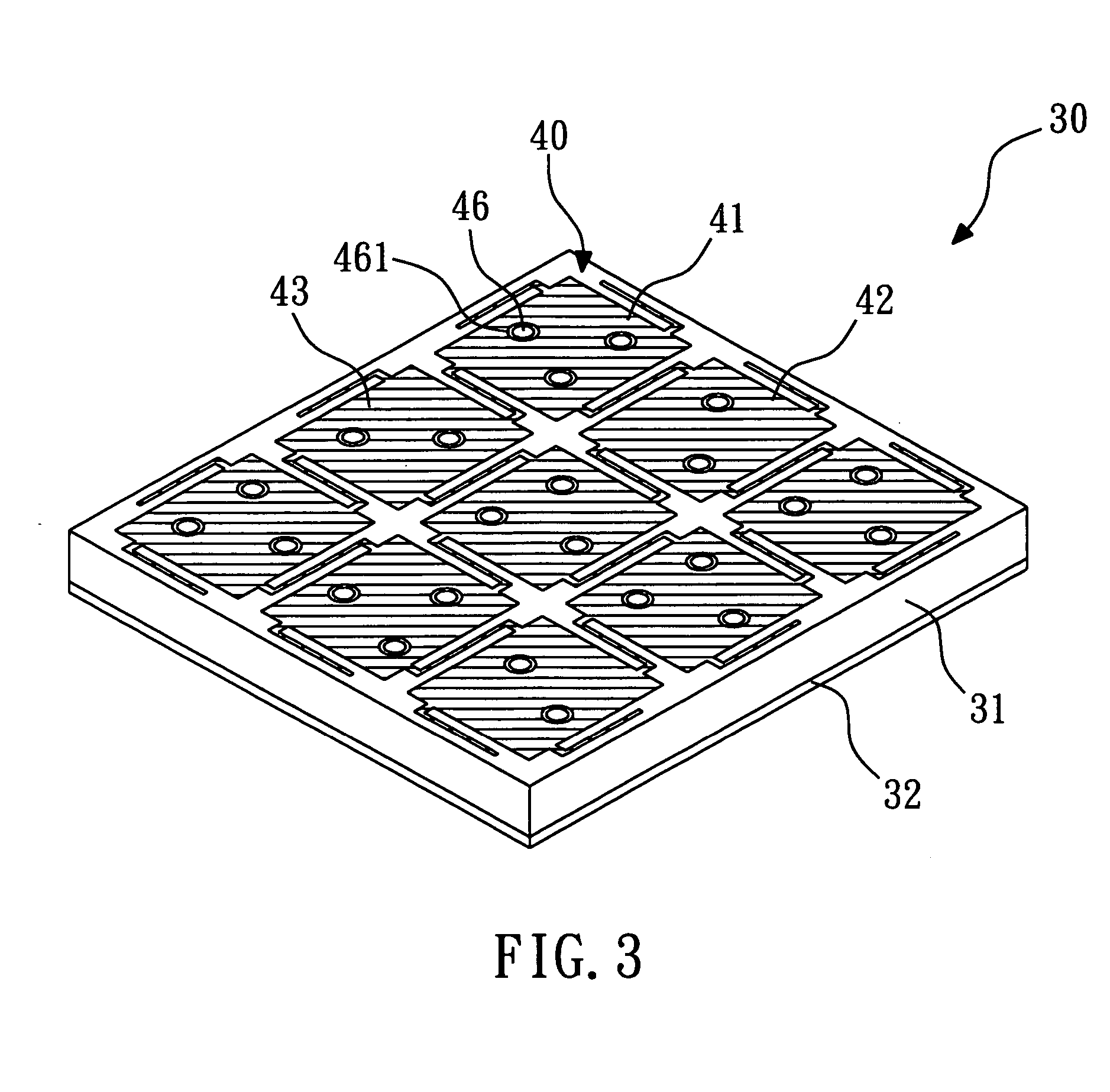
[0025] Referring to FIG. 3, according to the invention, a power plane system 30 of the invention comprises a substrate 31, a power layer 40 and a ground layer 32. The substrate 31 comprises a first surface and a second surface corresponding to the first surface. The power layer 40 is formed on the first surface of the substrate 31. The ground layer 32 is formed on the second surface of the substrate 31, and the ground layer 32 is a grounding metal plate. The power plane system of the invention can be applied to multi-layer structure, thus the power layer and the ground layer are not limited to be formed on the same structure and can be formed on different substrates.

[0026] The substrate may be a printed circuit board to apply the power plane system of the invention to multi-layer printed circuit board structure. Besides, the substrate may be a semiconductor packaging substrate to apply the power plane system of the invention to multi-layer semiconductor packaging structure. Furtherm...

fourth embodiment

[0037] Referring to FIG. 8, according to the invention, a power plane system 80 of the invention comprises a substrate 81, a power layer 90 and a ground layer 82. The substrate 81 comprises a first surface and a second surface corresponding to the first surface. The power layer 90 is formed on the first surface of the substrate 81. The ground layer 82 is formed on the second surface of the substrate 81, and the ground layer 82 is a grounding metal plate.

[0038] Referring to FIG. 9, the power layer 90 has a plurality of metal units 91, 92, 93 and a plurality of unit slits 96. The unit slit is spaced apart the adjacent metal units. For example, the unit slit 96 is spaced apart the adjacent metal units 91 and 92. Referring to FIG. 10, the metal unit 91 is taken as an example for illustration. The metal unit 91 comprises a metal unit plate 911 and a plurality of channels 912, 913. The channels 912, 913 are used for electrically connecting the metal unit 91 and the adjacent metal units. F...


PUM


Abstract

The invention relates to a power plane system for suppressing ground bounce noise. The power plane system of the invention comprises a substrate, a power layer and a ground layer. The power layer comprises a plurality of metal units. There is a distance between two adjacent metal units. A plurality of bridges is used for connecting the metal units. The ground layer has a grounding metal plate. According to the invention, when the ground bounce noise occurs, the metal units can broaden the stop-band bandwidth. Therefore, the signals in the stop-band hardly are transmitted so as to suppress the ground bounce noise, and the high frequency ground bounce noise and the electromagnetic radiation can be suppressed efficiently.

Description

BACKGROUND OF THE INVENTION [0001] 1. Field of the Invention [0002] The present invention relates to a power plane system of high-speed digital circuit, more particularly, a power plane system of high-speed digital circuit for suppressing ground bounce noise. [0003] 2. Description of the Related Art [0004] The related prior art has been disclosed in U.S. Pat. Nos. 6,084,779, 6,557,154 and 6,518,930. [0005] In high-speed digital circuit, signal line connects to the power plane, and there are parasitic inductance, capacitance and resistance. When the integrated circuit rapidly switches, a temporary voltage (ΔV) is produced between the power plane. The temporary voltage is a noise known as ground bounce noise (GBN). The resonance mode excited by the ground bounce noise causes significant signal integrity (SI) problem and electromagnetic interference (EMI) issues. [0006] Two conventional techniques are utilized to decrease the influence of the ground bounce noise. Firstly, adding decoup...

Claims


Application Information

Patent Timeline
IPC IPC(8): H01L23/50H01L23/552H03K17/16H03K19/003H05K1/02
CPCH01L23/50H01L23/552H01L2924/3011H05K1/0216H05K2201/09263H05K2201/093H01L2924/0002H05K2201/09309H05K2201/09663H01L2924/00
Inventor WU, TZONG-LINLIN, YEN-HUICHEN, SIN-TINGWANG, TING-KUANG
Owner NAT SUN YAT SEN UNIV
Why Eureka
Try Eureka