Dies bonding apparatus and dies bonding method

a dies bonding and dies technology, applied in the direction of packaging goods, paper/cardboard containers, transportation and packaging, etc., to achieve the effect of enhancing the effect of causing air between the chip and the chip mounting surface to escape to the outside and simple method

Inactive Publication Date: 2005-08-11
OKI ELECTRIC IND CO LTD
View PDF3 Cites 32 Cited by
  • Summary
  • Abstract
  • Description
  • Claims
  • Application Information

AI Technical Summary

Benefits of technology

[0054] According to the dies bonding method of the present invention, the amount of the adhesive agent directed from the central portion to the outside becomes greater than the amount thereof from the outside to the center. Therefore, the area wet by the adhesive agent of the central portion is ensured and the effect of ca

Problems solved by technology

However, the bonding apparatus or bonding method disclosed in the above document encounters difficulties in applying a bonding agent to the whole rectangular

Method used


Image

  • Dies bonding apparatus and dies bonding method
  • Dies bonding apparatus and dies bonding method
  • Dies bonding apparatus and dies bonding method

Examples


first embodiment

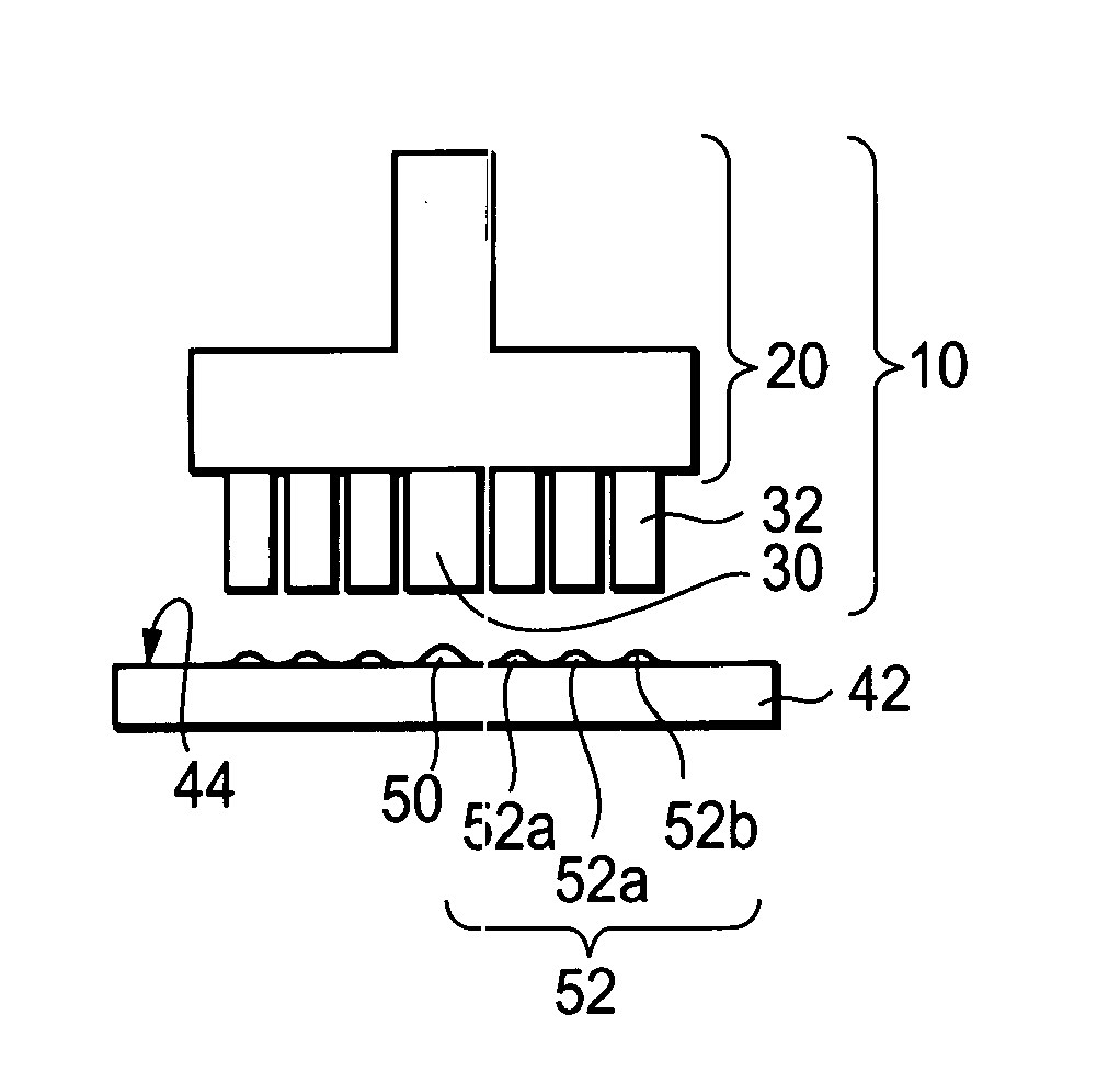
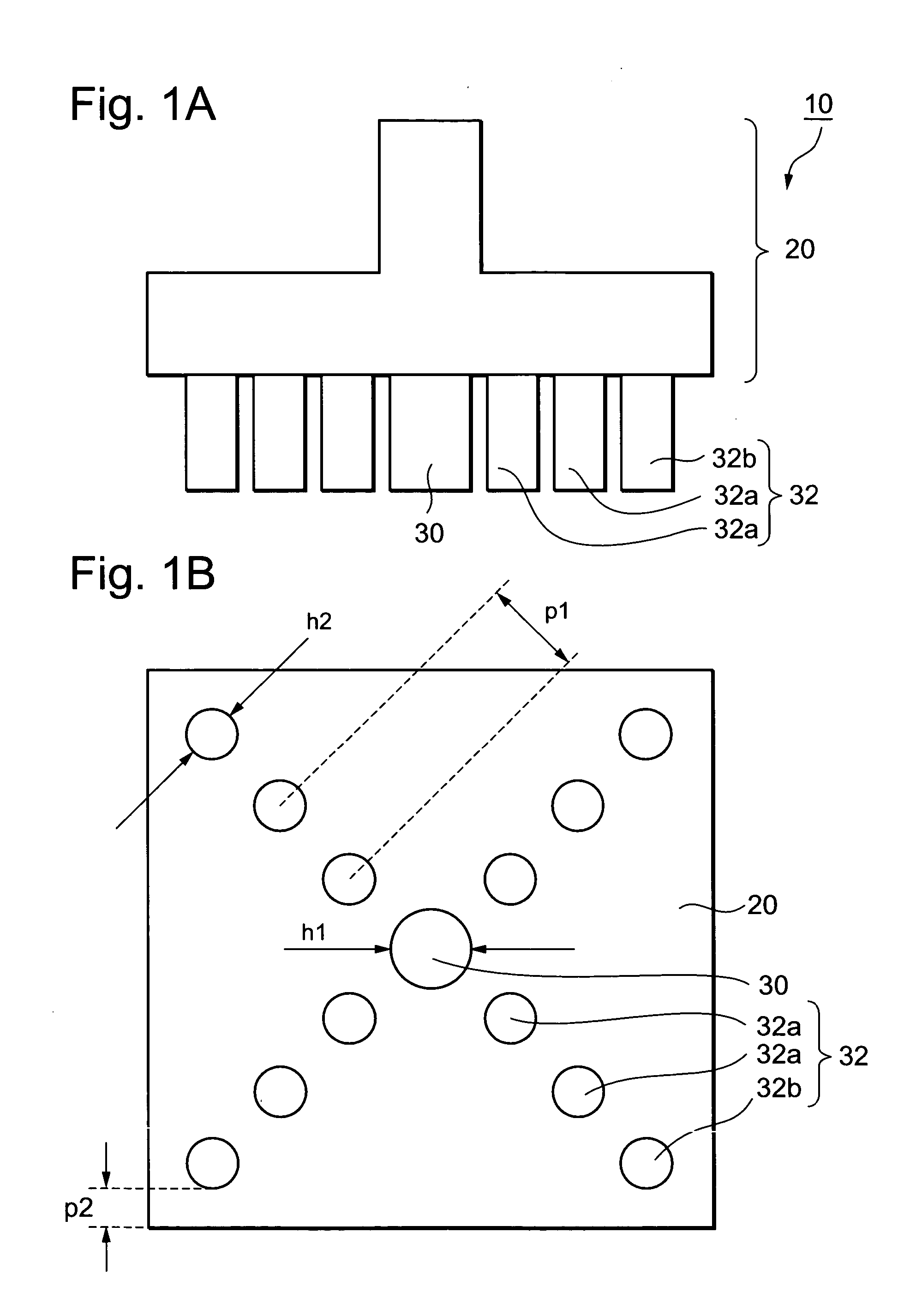
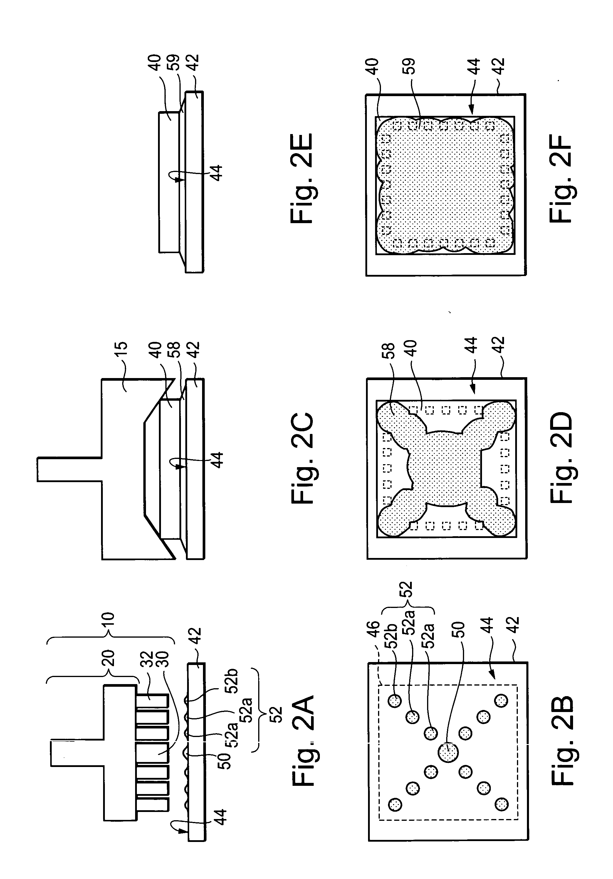
[0074] A dies bonding apparatus and a dies bonding method according to a first embodiment will be explained with reference to FIGS. 1(A) and 1(B) and FIGS. 2(A) through 2(F). FIGS. 1(A) and 1(B) are respectively views for describing the shape of a nozzle unit of the dies bonding apparatus. FIG. 1(A) is a schematic side view of the nozzle unit as viewed from its transverse direction with respect to the direction of discharge of adhesive agents. FIG. 1(B) is a schematic bottom view of the nozzle unit as viewed from below, i.e., from a chip mounting surface onto which the adhesive agents are applied. FIGS. 2(A) through 2(F) are views for describing the dies bonding method.

[0075] The dies bonding apparatus according to the first embodiment of the present invention includes a non-rotation type nozzle unit 10 and a pressing unit 15. The nozzle unit 10 discharges an adhesive agent to a bonding area of the chip mounting surface. The bonding area may be rectangular and is shaped in the form...

second embodiment

[0089] A dies bonding apparatus and a dies bonding method according to a second embodiment will be explained with reference to FIG. 4 and FIGS. 5(A) and 5(B). FIG. 4 is a view for describing the shape of a nozzle unit of the dies bonding apparatus and is a schematic bottom view of the nozzle unit as viewed from below, i.e., from a chip mounting surface on which an adhesive agent is applied. FIGS. 5(A) and 5(B) are respectively views for describing the dies bonding method.

[0090] The dies bonding apparatus according to the second embodiment of the present invention includes a non-rotation type nozzle unit 12 which delivers or discharges an adhesive agent to a bonding area of a chip mounting surface, which is rectangular, and a pressing unit (not shown) which uniformly and widely applies the adhesive agent to within the surface of the bonding area while a chip is being pressed against the chip mounting surface to which the adhesive agent is bonded. The pressing unit may have the funct...


PUM

PropertyMeasurementUnit
Diameteraaaaaaaaaa
Diameteraaaaaaaaaa
Diameteraaaaaaaaaa

Abstract

A dies bonding apparatus is provided with a nozzle unit for supplying an adhesive agent to a rectangular bonding area of a chip mounting surface. The nozzle unit includes a central nozzle for discharging an adhesive agent to the center of the bonding area, and a plurality of peripheral nozzles provided around the central nozzle and whose amount of discharge of the adhesive agent is smaller than the amount of discharge of the adhesive agent from the central nozzle.

Description

BACKGROUND OF THE INVENTION [0001] 1. Field of the Invention [0002] The present invention relates to a dies bonding apparatus and a dies bonding method. [0003] This application is counterparts of Japanese patent application, Serial Number 29857 / 2004, filed February 5, the subject matter of which is incorporated herein by reference. [0004] 2. Description of the Related Art [0005] When a semiconductor chip is bonded to a lead frame or a substrate or semiconductor chips are bonded to each other, the bonding quality of the semiconductor chip exerts an influence on the reliability of a semiconductor. In order to improve the reliability, there is a need to apply a bonding agent to the whole bonding area of the semiconductor chip. The semiconductor chip is hereinafter called simply “chip”. [0006] When a bonding agent is applied onto one point of a central portion and a rectangular chip is bonded to a substrate or the like, the bonding agent is expanded or spread in circular form. Therefore...

Claims


Application Information

Patent Timeline
IPC IPC(8): H01L21/52B05B1/14B05C5/00B05C5/02B65B1/00B65C1/00H01L21/00H01L21/44H01L21/58
CPCB05B1/14Y10T156/10H01L21/6715H01L24/27H01L24/30H01L24/743H01L24/83H01L2224/3003H01L2224/30151H01L2224/743H01L2224/83192H01L2224/83194H01L2224/8385H01L2924/01005H01L2924/01082H01L2924/07802H01L2924/01006H01L2924/01023H01L2924/01033H01L24/29B05C5/0208H01L2924/00
Inventor SUZUKI, SHINSUKEMURAKI, SHINJI
Owner OKI ELECTRIC IND CO LTD
Why Eureka
Try Eureka