

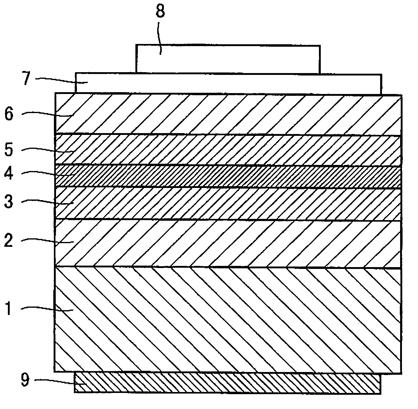
Nitride semiconductor devices and method of their manufacture
- Summary
- Abstract
- Description
- Claims
- Application Information
AI Technical Summary
Benefits of technology
Problems solved by technology
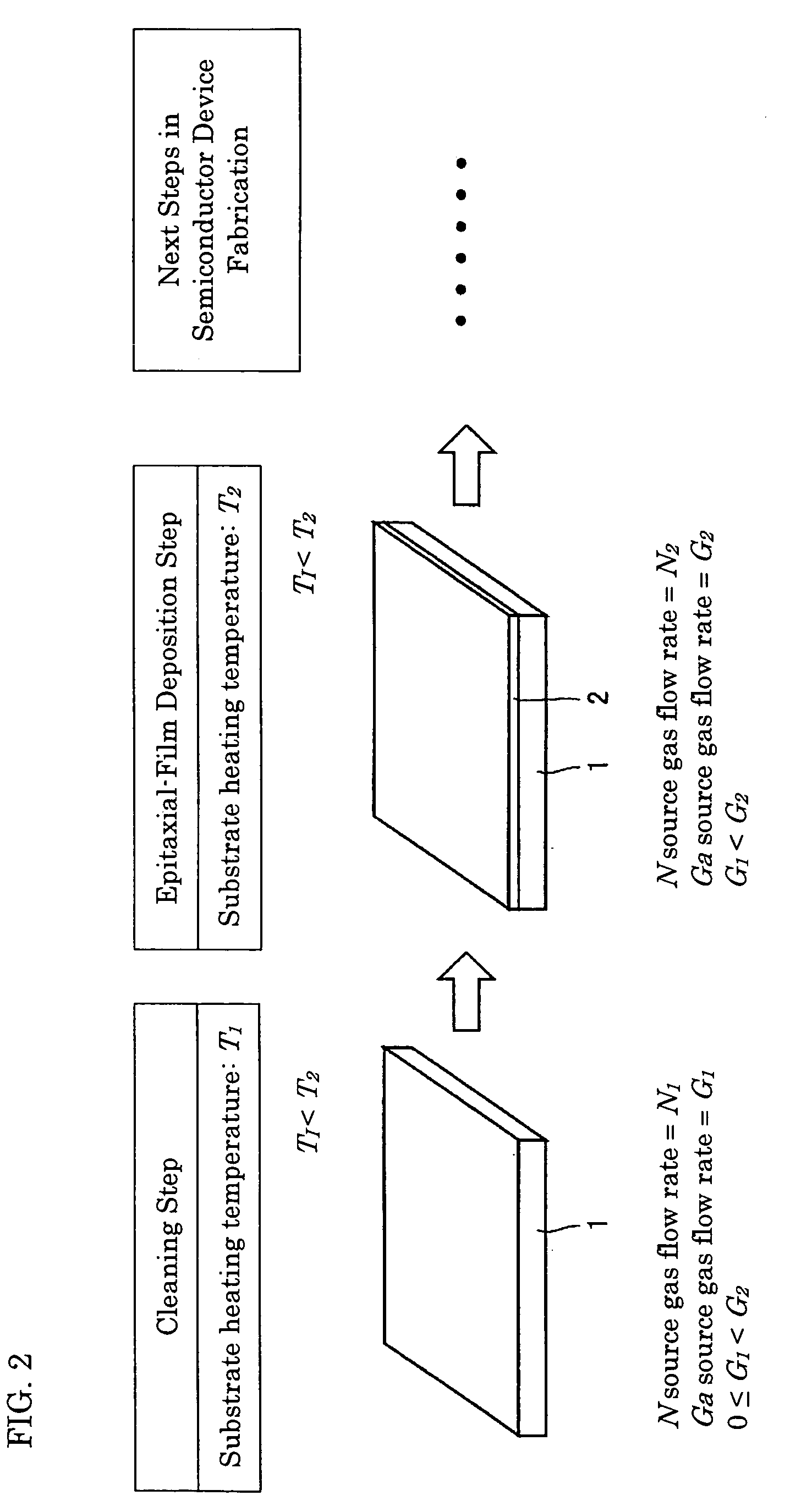
Method used
Image

Examples
Example
[0051] Comparative example: 1150° C.
[0052] Pretreating time—10 minutes
Film-Deposition Conditions
[0053] Nitrogen: 20 slm
[0054] Hydrogen: 15 slm
[0055] Ammonia: 5 slm
[0056] TMG: 19 sccm
[0057] Substrate temperature—1150° C.
[0058] Utilized as the GaN substrate was a bulk crystal prepared by growing a thick GaN film onto a GaAs substrate with SiO2 made the mask and thereafter removing the GaAs substrate. (Cf. PCT Gazette Pub. No. WO99 / 23693.) In the pretreatment, the Ga source gas TMG was omitted, and ammonia as the nitrogen source gas, and nitrogen and hydrogen as the carrier gases alone were flowed according to the same flow parameters as those in the film-deposition conditions noted above. The root-mean-square (RMS) roughness of the substrate after having undergone the pretreatment was assessed using atomic force microscopy (AFM).
[0059]FIG. 3 is micrographs made using AFM, showing 10 μm×10 μm of roughness, for RMS calculations, along the front side of the GaN substrate. The v...
PUM
| Property | Measurement | Unit |
|---|---|---|
| Height | aaaaa | aaaaa |
| Height | aaaaa | aaaaa |
| Height | aaaaa | aaaaa |
Abstract
Description
Claims
Application Information